Max8730 low-cost battery charger – Rainbow Electronics MAX8730 User Manual
Page 27
MAX8730
Low-Cost Battery Charger
______________________________________________________________________________________
27
For typical applications, choose t
Delay
= 20µs
(depends on the p-MOSFET selected for the PDS
switch).
The following components can be used for a 10A sys-
tem short-current design:
R10 = 8.66k
Ω
C6 = 0.1µF
R15 = 7.15k
Ω
C13 = 2.7nF
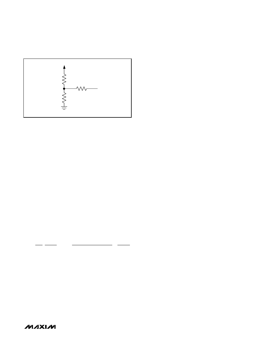
Foldback Current
At low duty cycles, most of the charge current is con-
ducted through the Schottky diode (D1). To reduce the
requirements of the Schottky diode, the MAX8730 has a
foldback charge current feature. When the battery volt-
age falls below 5 x V
RELTH
, ICTL sinks 6µA. Add a
series resistor to ICTL to adjust the charge current fold-
back, as shown in Figure 12:
Layout and Bypassing
Bypass SRC, ASNS, LDO, DHIV, and REF as shown in
Figure 1.
Good PC board layout is required to achieve specified
noise immunity, efficiency, and stable performance.
The PC board layout artist must be given explicit
instructions—preferably, a sketch showing the place-
ment of the power-switching components and high-
current routing. Refer to the PC board layout in the
MAX8730 evaluation kit for examples.
Use the following step-by-step guide:
1) Place the high-power connections first, with their
grounds adjacent:
• Minimize the current-sense resistor trace lengths,
and ensure accurate current sensing with Kelvin
connections.
• Minimize ground trace lengths in the high-current
paths.
• Minimize other trace lengths in the high-current
paths.
• Use > 5mm wide traces in the high-current
paths.
• Connect to the input capacitors directly to the
source of the high-side MOSFET (10mm max
length). Place the input capacitor between the
input current-sense resistor and the source of the
high-side MOSFET.
2) Place the IC and signal components. Quiet connec-
tions to REF, CCV, CCI, CCS, ACIN, SWREF, and
LDO SRC should be returned to a separate ground
(GND) island. There is very little current flowing in
these traces, so the ground island need not be very
large. When placed on an inner layer, a sizable
ground island can help simplify the layout because
the low current connections can be made through
vias. The ground pad on the backside of the pack-
age should be the star connection to this quiet
ground island.
3) Keep the gate drive trace (DHI) and SRC path as
short as possible (L < 20mm), and route them away
from the current-sense lines and REF. Bypass DHIV
directly to the source of the high-side MOSFET.
These traces should also be relatively wide (W >
1.25mm).
4) Place ceramic bypass capacitors close to the IC.
The bulk capacitors can be placed further away.
R
A
R
R
R
x V
I
x RS x
V
mV
R x R
R
R
REF
FOLDBACK
14
1
6
8
7
8
2
3 6
135
8
7
7
8
=
+
−
−
+
µ
.
REF
R7
R8
R14
ICTL
Figure
12. ICTL Foldback Current Adjustment