Max8730 low-cost battery charger, Pin description – Rainbow Electronics MAX8730 User Manual
Page 14
MAX8730
Low-Cost Battery Charger
14
______________________________________________________________________________________
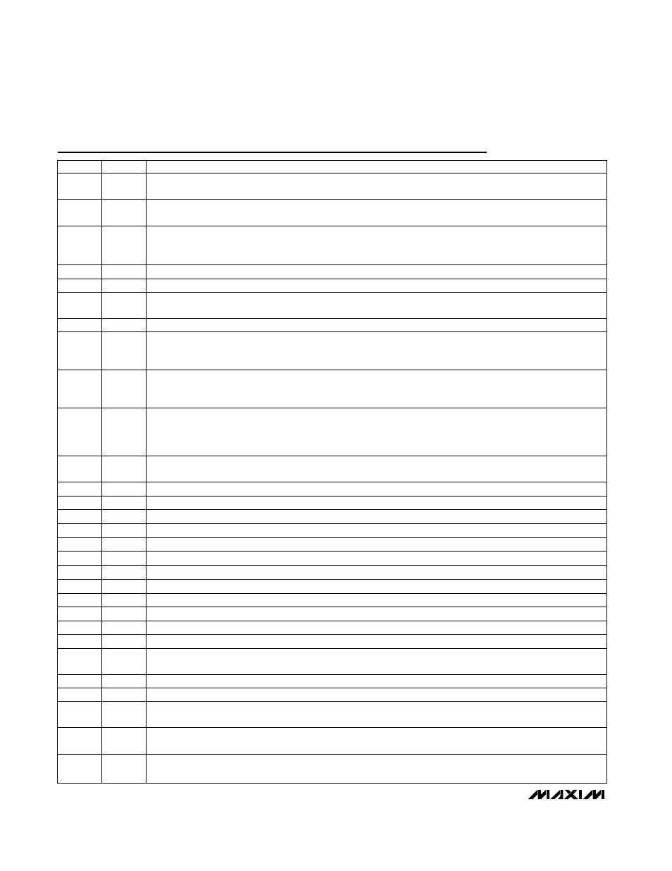
PIN
NAME
FUNCTION
1
ASNS
Adapter Voltage Sense. When V
ASNS
> V
BATT
- 280mV, the battery switch is turned off and the adapter switch
is turned on. Connect to the adapter input using an RC filter as shown in Figure 1.
2
LDO
Linear-Regulator Output. LDO is the output of the 5.35V linear regulator supplied from SRC. Bypass LDO with
a 1µF ceramic capacitor from LDO to GND.
3
SWREF
3.3V Switched Reference. SWREF is a 1% accurate linear regulator that can deliver 20mA. SWREF remains
active when the adapter is absent and may be disabled by setting REFON to zero. Bypass SWREF with a 1µF
capacitor to GND.
4
REF
4.2V Voltage Reference. Bypass REF with a 1µF capacitor to GND.
5
CLS
Source Current-Limit Input. Voltage input for setting the current limit of the input source.
6
ACIN
AC-Adapter-Detect Input. ACIN is the input to an uncommitted comparator. ACIN does not influence adapter
and battery selection.
7
VCTL
Charge-Voltage-Control Input. Connect VCTL to LDO for default 4.2V/cell.
8
RELTH
Relearn Threshold for Relearn Mode. In relearn mode, when V
BATT
< 5 x V
RELTH
, the MAX8730 drives PDS
low and drives PDL high to terminate relearning of a discharged battery. See the Relearn Mode section for
more details.
9
ACOK
AC Detect Output. This open-drain output pulls low when ACIN is greater than REF/2 and ASNS is greater
than BATT - 100mV. The ACOK output is high impedance when the MAX8730 is powered down. Connect a
10k
Ω pullup resistor from LDO to ACOK.
10
MODE
Tri-Level Input for Setting Number of Cells or Asserting the Conditioning Mode:
MODE = GND; asserts relearn mode.
MODE = Float; charge with 3 times the cell voltage programmed at VCTL.
MODE = LDO; charge with 4 times the cell voltage programmed at VCTL.
11
IINP
Input-Current-Monitor Output. IINP sources the current proportional to the current sensed across CSSP and
CSSN. The transconductance from (CSSP – CSSN) to IINP is 2.8µA/mV (typ).
12
ICTL
Charge-Current-Control Input. Pull ICTL to GND to shut down the charger.
13
REFON
SWREF Enable. Drive REFON high to enable SWREF.
14
INPON
Input Current-Monitor Enable. Drive INPON high to enable IINP.
15
CCI
Output Current-Regulation Loop Compensation Point. Connect a 0.01µF capacitor from CCS to GND.
16
CCV
V ol tag e- Reg ul ati on Loop C om p ensati on P oi nt. C onnect a 10k
Ω r esi stor i n ser i es w i th a 0.01µF cap aci tor to G N D .
17
CCS
Input Current-Regulation Loop Compensation Point. Connect a 0.01µF capacitor from CCS to GND.
18
GND
Analog Ground
19
BATT
Battery-Voltage Feedback Input
20
CSIN
Charge-Current-Sense Negative Input
21
CSIP
Charge-Current-Sense Positive Input. Connect a current-sense resistor from CSIP to CSIN.
22
DHIV
High-Side Driver Supply. Connect a 0.1µF capacitor from DHIV to CSSN.
23
DHI
High-Side Power MOSFET Driver Output. Connect to high-side, p-channel MOSFET gate.
24
SRC
DC Supply Input Voltage and Connection for Driver for PDS/PDL Switches. Bypass SRC to power ground with
a 1µF capacitor.
25
CSSN
Input Current Sense for Negative Input
26
CSSP
Input Current Sense for Positive Input. Connect a 15m
Ω current-sense resistor from CSSP to CSSN.
27
PDS
Power-Source PMOS Switch Driver Output. When the adapter is absent, the PDS output is pulled to SRC
through an internal 1M
Ω resistor.
28
PDL
System-Load PMOS Switch Driver Output. When the adapter is absent, the PDL output is pulled to ground
through an internal 100k
Ω resistor.
29
Backside
Paddle
Backside Paddle. Connect the backside paddle to analog ground.
Pin Description