Max8730 low-cost battery charger, Design procedure, Table 3. recommended mosfets – Rainbow Electronics MAX8730 User Manual
Page 24
MAX8730
Low-Cost Battery Charger
24
______________________________________________________________________________________
MOSFET Drivers
The DHI output is optimized for driving moderate-sized
power MOSFETs. This is consistent with the variable
duty factor that occurs in the notebook computer envi-
ronment where the battery voltage changes over a wide
range. DHI swings from SRC to DHIV and has a typical
impedance of 1
Ω sourcing and 4Ω sinking.
Design Procedure
MOSFET Selection
Choose the p-channel MOSFETs according to the max-
imum required charge current. The MOSFET (P4) must
be able to dissipate the resistive losses plus the switch-
ing losses at both V
SRC(MIN)
and V
SRC(MAX)
.
The worst-case resistive power losses occur at the
maximum battery voltage. Calculate the resistive losses
according to the following equation:
Calculate the switching losses according to the follow-
ing equation:
where C
RSS
is the reverse transfer capacitance of the
MOSFET, and I
GATE
is the peak gate-drive source/sink
current.
These calculations provide an estimate and are not a
substitute for breadboard evaluation, preferably includ-
ing a verification using a thermocoupler mounted on
the MOSFET.
Generally, a small MOSFET is desired to reduce switch-
ing losses at V
BATT
= V
SRC
/ 2. This requires a tradeoff
between gate charge and resistance. Switching losses
in the MOSFET can become significant when the maxi-
mum AC adapter voltage is applied. If the MOSFET that
was chosen for adequate R
DS(ON)
at low supply volt-
ages becomes hot when subjected to V
SRC(MAX)
, then
choose a MOSFET with lower gate charge. The actual
switching losses that can vary due to factors include
the internal gate resistance, threshold voltage, source
inductance, and PC board layout characteristics.
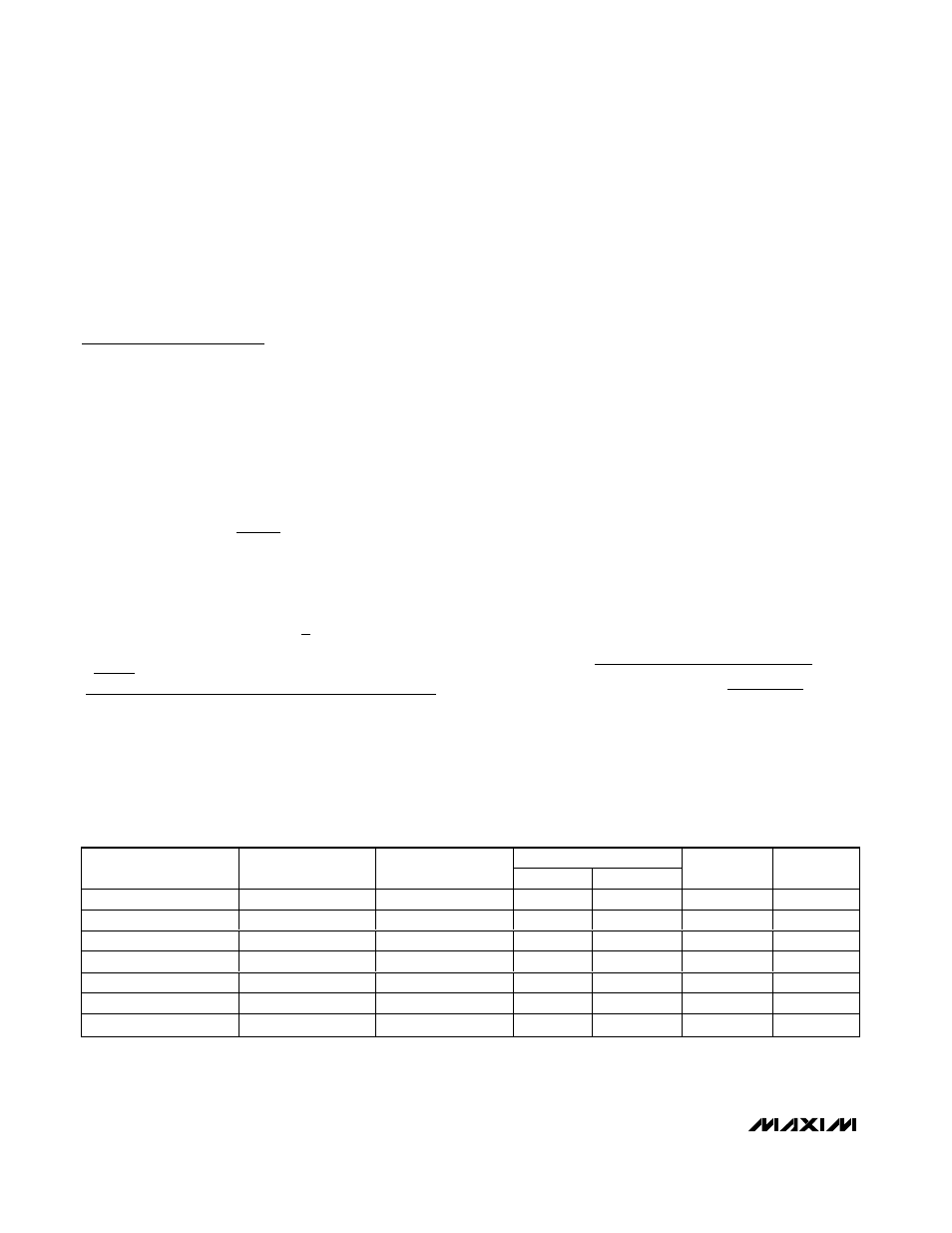
See Table 3 for suggestions about MOSFET selection.
Schottky Selection
The Schottky diode conducts the inductor current dur-
ing the off-time. Choose a Schottky diode with the
appropriate thermal resistance to guarantee that it does
not overheat:
θ
JA
J MAX
A MAX
F
CHG
BATT MIN
SRC MAX
T
T
V
x I
x
V
V
_
_
_
_
<
−
−
1
PD
x
xQ
I
x V
I
V
C
f
SWITCHING
G
GATE
SRC MAX x CHG
SRC MAX
x
RSS
(
)
(
)
=
+
(
)
1
2
2
2
PD
V
V
x I
R
sis
ce
BATT
SRC
CHG
DS ON
Re
tan
(
)
=
×
2
Table 3. Recommended MOSFETs
MAX
CHARGE CURRENT (A)
MOSFET
PIN-PACKAGE
Q
G
(nC)
R
DSON
(m
Ω)
R
θθθθ
JA
(°/W)
T
MAX
(°C)
3
Si3457DV
6-SOT23
8
75
78
+150
2.5
FDC658P
6-SOT23
12
75
78
+150
3.5
FDS9435A
8-SO
14
80
50
+175
3.5
NDS9435A
8-SO
14
80
50
+175
4
FDS4435
8-SO
24
35
50
+175
4
FDS6685
8-SO
24
35
50
+175
4.5
FDS6675A
8-SO
34
19
50
+175