Max8730 low-cost battery charger – Rainbow Electronics MAX8730 User Manual
Page 22
MAX8730
Low-Cost Battery Charger
22
______________________________________________________________________________________
where:
V
BATT
= 16.8V
GMV = 0.125µA/mV
GM
OUT
= 2.22A/V
C
OUT
= 10µF
f
OSC
= 350kHz (minimum occurs at V
IN
= 19V and
V
BATT
= 16.8V)
R
L
= 0.2
Ω
f
CO-CV
= 45kHz
To ensure that the compensation zero adequately can-
cels the output pole, select f
Z_CV
≤ f
P_OUT
:
C
CV
≥ (R
L
/ R
CV
) C
OUT
C
CV
≥ 200pF
Figure 5 shows the Bode plot of the voltage-loop fre-
quency response using the values calculated above.
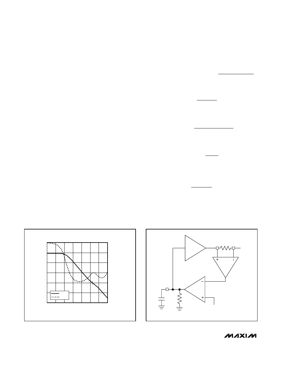
CCI Loop Compensation
The simplified schematic in Figure 6 is sufficient to
describe the operation of the MAX8730 when the bat-
tery current loop (CCI) is in control. Since the output
capacitor’s impedance has little effect on the response
of the current loop, only a simple single pole is required
to compensate this loop. A
CSI
is the internal gain of the
current-sense amplifier. RS2 is the charge-current-
sense resistor (30m
Ω). R
OGMI
is the equivalent output
impedance of the GMI amplifier, which is greater than
10M
Ω. GMI is the charge-current amplifier transcon-
ductance = 1µA/mV. GM
OUT
is the DC-DC converter
transconductance = 2.22A/V.
The loop transfer function is given by:
that describes a single-pole system. Since:
the loop-transfer function simplifies to:
The crossover frequency is given by:
For stability, choose a crossover frequency lower than
1/10 of the switching frequency:
Values for C
CI
greater than 10 times the minimum value
may slow down the current-loop response. Choosing
C
CI
= 10nF yields a crossover frequency of 15.9kHz.
Figure 7 shows the Bode plot of the current-loop fre-
quency response using the values calculated above.
C
x GMI
x C
nF
CI
CI
>
=
10
2
4
π
f
GMI
C
CO CI
CI
_
=
2
π
LTF
GMI
R
sR
C
OGMI
OGMI
CI
=
+
×
1
GM
A
RS
OUT
CSI
=
×
1
LTF
GM
A
RS
GMI
R
sR
C
OUT
CSI
OGMI
OGMI
CI
=
Ч
Ч
Ч
+
Ч
1
FREQUENCY (Hz)
MAGNITUDE (dB)
PHASE (DEGREES)
100k
10k
1k
100
10
1
-20
0
20
40
60
80
-40
-90
-45
0
-135
0.1
1M
MAG
PHASE
Figure 5. CCV Loop Response
C
CI
R
OGMI
CCI
GMI
CSI
ICTL
GM
OUT
CSIP
RS2
CSIN
Figure 6. CCI Loop Diagram