Typical operating circuit chip information – Rainbow Electronics MAX6973 User Manual
Page 21
MAX6972/MAX6973
16-Output PWM LED Drivers
for Message Boards
______________________________________________________________________________________
21
Power-Supply Considerations
The MAX6972/MAX6973 operate with a power-supply
voltage of 3.0V to 3.6V. Bypass the V
DD
power supply
to GND with a 0.1µF ceramic capacitor as close as
possible to the device pins. If the LED supply is shared
with the V
DD
supply, adequately decouple the V
DD
supply with bulk capacitance to ensure that the fast-
rising, high-current LED drive currents do not cause
transient dips in V
DD
.
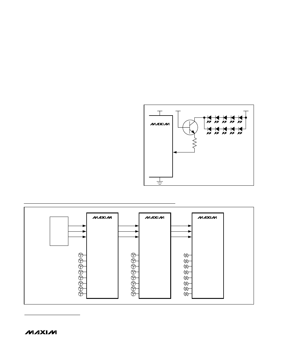
Driving LEDs from a Supply Higher than 7V
An external npn transistor in a cascode configuration
extends the output drive voltage above 7V. The external
pass transistor’s emitter clamps to a V
BE
below its
base, which is connected to the MAX6972/MAX6973’s
supply voltage. An optional emitter resistor reduces the
voltage drop across the MAX6972/MAX6973’s output
transistor and effectively takes the dissipation off the
device into the resistor. The external transistor’s collector
current is equal to its emitter current (less a small base
current), and the MAX6972/MAX6973 accurately
control the emitter current with a constant current sink
driver structure.
Example of using an external npn transistor:
V
DD
= 3.3V ±5%, I
OUT
= 55mA, external pass transistor
V
BE
= 0.7V - 1V at 55mA emitter current.
For best output current accuracy, design V
O
to be at
least 1.2V:
R1
(MAX)
= (3.15 - 1 - 1.2) / 0.055 = 17.3
Ω, so choose
R1 = 15
Ω
hence,
V
O(MIN)
= 3.15 - 1 - (15 x 0.055) = 1.325V and V
O(MAX)
= 3.45 - 0.7 - (15 x 0.055) = 1.925V.
MAX6972
MAX6973
V
DD
R1
Q1
55mA
+3.3V
+3.3V
+24V
Y1
Y2
Y3
Y4
Y5
Y6
Y7
Y0
GND
Figure 13. External Cascode npn Transistor
MAX6972
MAX6972
MAX6972
SYSTEM
CLK
DATA
LOAD
CLKO
DINO
LOADO
CLKI
DINI
LOADI
Y0/Z0
16 RG LEDs
16 BLUE LEDs
Y1/Z1
Y2/Z2
Y3/Z3
Y4/Z4
Y5/B5
Y6/Z6
Y7/Z7
Y0/Z0
Y1/Z1
Y2/Z2
Y3/Z3
Y4/Z4
Y5/B5
Y6/Z6
Y7/Z7
Y0/Z0
Y1/Z1
Y2/Z2
Y3/Z3
Y4/Z4
Y5/B5
Y6/Z6
Y7/Z7
CLKO
DINO
LOADO
CLKI
DINI
LOADI
CLKO
DINO
LOADO
CLKI
DINI
LOADI
Typical Operating Circuit
Chip Information
PROCESS: BiCMOS