Absolute maximum ratings, Electrical characteristics – Rainbow Electronics MAX6973 User Manual
Page 2
MAX6972/MAX6973
16-Output PWM LED Drivers
for Message Boards
2
_______________________________________________________________________________________
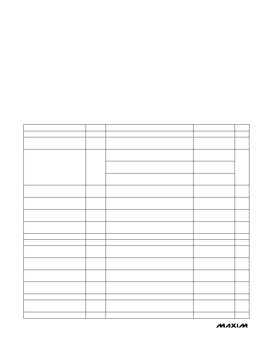
ABSOLUTE MAXIMUM RATINGS
Stresses beyond those listed under “Absolute Maximum Ratings” may cause permanent damage to the device. These are stress ratings only, and functional
operation of the device at these or any other conditions beyond those indicated in the operational sections of the specifications is not implied. Exposure to
absolute maximum rating conditions for extended periods may affect device reliability.
(All voltages with respect to GND.)
V
DD
........................................................................-0.3V to +4.0V
Y0–Y7, Z0–Z7, MUX0, and MUX1 .........................-0.3V to +8.0V
All Other Pins..............................................-0.3V to (V
DD
+ 0.3V)
Continuous Power Dissipation (T
A
= +70°C)
32-Pin TQFN (derate 34.5mW/°C over +70°C) ..........2857mW
Operating Temperature Range .........................-40°C to +125°C
Junction Temperature ......................................................+150°C
Storage Temperature Range .............................-65°C to +150°C
Lead Temperature (soldering, 10s) .................................+300°C
PARAMETER
SYMBOL
CONDITIONS
MIN
TYP
MAX
UNITS
Operating Supply Voltage
V
DD
3.0
3.6
V
LEDs Anode Voltage
(Y0–Y7, Z0–Z7, MUX0, and MUX1)
V
O
7
V
f
CLKI
= 0Hz; CLKO_, DOUT_ loaded 200
Ω;
calibration DACs set to 0x01
21
35
f
CLKI
= 0Hz; CLKO_, DOUT_ loaded 200
Ω;
calibration DACs set to 0xFF
40
55
Supply Current
I
DD
f
CLKI
= 32MHz; CLKO_, DOUT_ loaded 200
Ω;
calibration DACs set to 0xFF
42
60
mA
Input High Voltage LOADI
V
IHC
0.7
x V
DD
V
Input Low Voltage LOADI
V
ILC
0.3
x V
DD
V
Differential Input Voltage Range
CLKI_, DIN_
V
ID
±0.15
±1.20
V
Common-Mode Input Voltage
CLKI_, DIN_
V
CM
| V
I D
/ 2|
2.4
V
Differential Input High Threshold
VDIFF
TH
8
65
mV
Differential Input Low Threshold
VDIFF
TL
-65
-8
mV
Differential Output Voltage
CLKO_, DOUT_
V
OD
Termination 200
Ω at receiver _+ and _- inputs
±190
±550
mV
Differential Output Offset
CLKO_, DOUT_
V
OS
Termination 200
Ω at receiver _+ and _- inputs
1.125
1.25
1.375
V
Input Leakage Current
CLKI_, DIN_, LOADI
I
IH
, I
IL
-1
+1
µA
Input Capacitance
CLKI_, DIN_, LOADI
10
pF
Output Low Voltage LOADO
V
OLC
I
SINK
= 5mA
0.05
0.25
V
Output High Voltage LOADO
V
OHC
I
SOURCE
= 5mA
V
DD
- 0.5
V
DD
- 0.2
V
Output Slew Time LOADO
20% to 80%, 80% to 20%, load = 10pF
3
ns
ELECTRICAL CHARACTERISTICS
(V
DD
= 3.0V to 3.6V, T
A
= T
MIN
to T
MAX
, unless otherwise noted. Typical values are at V
DD
= 3.3V, T
A
= +85°C.) (Note 1)