Rainbow Electronics MAX13483E User Manual
Page 2
MAX13481E/MAX13482E/MAX13483E
±15kV ESD-Protected USB Transceivers with
External/Internal Pullup Resistors
2
_______________________________________________________________________________________
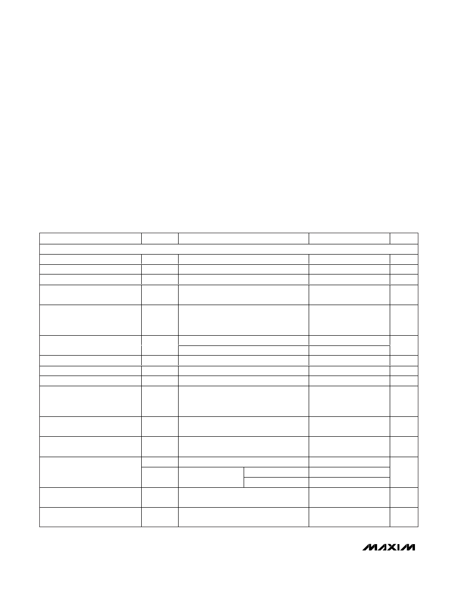
ABSOLUTE MAXIMUM RATINGS
ELECTRICAL CHARACTERISTICS
(V
CC
= +4V to +5.5V, V
L
= +1.6V to +3.6V, T
A
= T
MIN
to T
MAX
, unless otherwise noted. Typical values are at V
CC
= +5V, V
L
= +2.5V,
T
A
= +25°C.) (Note 1)
Stresses beyond those listed under “Absolute Maximum Ratings” may cause permanent damage to the device. These are stress ratings only, and functional
operation of the device at these or any other conditions beyond those indicated in the operational sections of the specifications is not implied. Exposure to
absolute maximum rating conditions for extended periods may affect device reliability.
(All voltages referenced to GND, unless otherwise noted.)
V
BUS
, V
L,
..................................................................-0.3V to +7V
V
TRM
, VPUR, VPU .....................................-0.3V to (V
BUS
+ 0.3V)
Input Voltage (D+, D-) ..............................................-0.3V to +7V
VM, VP, SUS, RCV,
ENUM, BD, OE, ............-0.3V to (V
L
+ 0.3V)
Short-Circuit Current to V
CC
or GND (D+, D-)… ........... ±150mA
Maximum Continuous Current (all other pins) ..................±15mA
Continuous Power Dissipation (T
A
= +70
°C)
16-Pin, 3mm x 3mm TQFN (derate 15.6mW/
°C above
+70
°C).......................................................................1250mW
Operating Temperature Range ...........................-40
°C to +85°C
Junction Temperature ......................................................+150
°C
Storage Temperature Range .............................-65
°C to +150°C
Lead Temperature (soldering, 10s) .................................+300
°C
PARAMETER
SYMBOL
CONDITIONS
MIN
TYP
MAX
UNITS
SUPPLY INPUTS (V
BUS
, V
TRM
, V
L
)
V
BUS
Input Range
V
BUS
4.0
5.5
V
V
L
Input Range
V
L
1.6
3.6
V
Regulated Supply-Voltage Output
V
VTRM
3.0
3.3
3.6
V
Operating V
CC
Supply Current
I
VCC
Full-speed transmitting/receiving at
12Mbps, C
L
= 50pF on D+ and D- (Note 2)
10
mA
Operating V
L
Supply Current
I
VL
Full-speed transmitting/receiving at
12Mbps, C
L
= 15pF receiver outputs,
V
L
= 2.5V (Note 2)
2.5
mA
Full-speed idle, V
D+
> 2.7V, V
D-
< 0.3V
250
350
Full-Speed Idle and SE0 Supply
Current
I
VCC(IDLE)
SE0: V
D+
< 0.3V, V
D-
< 0.3V
250
350
µA
Static V
L
Supply Current
I
VL(STATIC)
Full-speed idle, SE0 or suspend mode
5
µA
Suspend Supply Current
I
VCC(SUSP)
VM = VP = open,
ENUM = SUS = OE = high
35
µA
Disabled-Mode Supply Current
I
VCC(DIS)
V
L
= GND or open
20
µA
Sharing-Mode V
L
Supply Current
I
V L(S H ARIN G)
V
BUS
= GND or open,
OE = low,
VP = low or high, VM = low or high, SUS =
high,
ENUM = high
5
µA
Disable-Mode Load Current on
D+ and D-
I
D X (D IS ABLE )
V
L
= GND or open, V
D_
= 0 or 5.5V
5
µA
Sharing-Mode Load Current on
D+ and D-
I
DX (SH ARING)
V
BUS
= GND or open, V
D_
= 0 or 5.5V
20
µA
V
TH_H
Supply present
3.6
V
L
≥ 1.7V
0.8
USB Power-Supply Detection
Threshold
V
TH_L
Supply lost
V
L
< 1.7V
0.7
V
USB Power-Supply Detection
Hysteresis
V
HYST
75
mV
V
L
Supply-Voltage Detection
Threshold
V
TH(VL)
0.85
V