Rainbow Electronics MAX9877 User Manual
Page 2
MAX9877
Low RF Susceptibility, Mono Audio
Subsystem with DirectDrive Headphone Amplifier
2
_______________________________________________________________________________________
ABSOLUTE MAXIMUM RATINGS
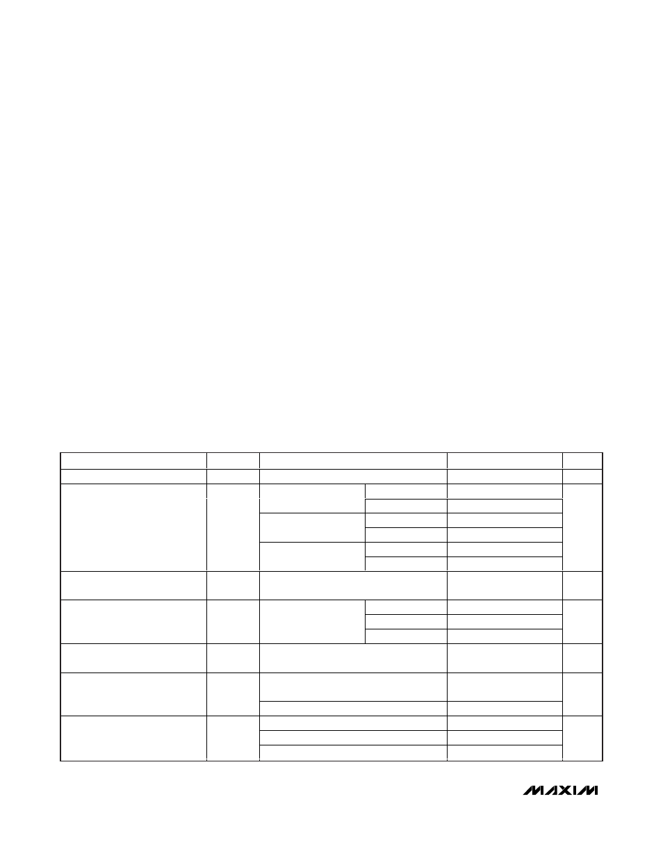
ELECTRICAL CHARACTERISTICS
(V
DD
= PV
DD
= 3.7V, V
GND
= V
PGND
= 0V. Single-ended inputs, preamp gain = 0dB, volume controls = 0dB, OSC = 00, BYPASS = 0,
SHDN = 1. Speaker loads (Z
SPK
) connected between OUT+ and OUT-. Headphone loads (R
HP
) connected from HPL or HPR to GND.
SDA and SCL pullup voltage = 3.3V. Z
SPK
=
∞, R
HP
=
∞. C1 = C2 = C
BIAS
= 1µF. T
A
= T
MIN
to T
MAX
, unless otherwise noted. Typical
values are at T
A
= +25°C.) (Note 3)
Stresses beyond those listed under “Absolute Maximum Ratings” may cause permanent damage to the device. These are stress ratings only, and functional
operation of the device at these or any other conditions beyond those indicated in the operational sections of the specifications is not implied. Exposure to
absolute maximum rating conditions for extended periods may affect device reliability.
Note 1: HPR and HPL should be limited to no more than 9V above V
SS
, or above PV
DD
+ 0.3V, whichever limits first.
Note 2: HPR and HPL should be limited to no more than 9V below PV
DD
, or below V
SS
- 0.3V, whichever limits first.
V
DD
, PV
DD
to PGND ..............................................-0.3V to +5.5V
V
DD
to PV
DD
..........................................................-0.3V to +0.3V
V
SS
to PGND .........................................................-5.5V to +0.3V
C1N to PGND..............................................(V
SS
- 0.3V) to +0.3V
C1P to PGND ...........................................-0.3V to (PV
DD
+ 0.3V)
HPL, HPR to V
SS
(Note 1) ......-0.3V to the lower of (PV
DD
- (V
SS
+ 0.3V)) or +9V
HPL, HPR to PV
DD
(Note 2) ......+0.3V to the higher of (V
SS
- (PV
DD
- 0.3V)) or -9V
GND to PGND.....................................................................±0.3V
INA1, INA2, INB1, INB2, BIAS..................................-0.3V to +4V
SDA, SCL...............................................................-0.3V to +5.5V
All Other Pins to GND...............................-0.3V to (PV
DD
+ 0.3V)
Continuous Current In/Out of PV
DD
, PGND, OUT_.........±800mA
Continuous Current In/Out of HPR and HPL .....................140mA
Continuous Current In/Out of RXIN+ and RXIN- ...............150mA
Continuous Input Current V
SS
...........................................100mA
Continuous Input Current (all other pins) .........................±20mA
Duration of OUT_ Short Circuit to GND or PV
DD
........Continuous
Duration of Short Circuit Between OUT+ and OUT- ..Continuous
Duration of HP_ Short Circuit to GND or PV
DD
..........Continuous
Continuous Power Dissipation (T
A
= +70°C)
20-Bump WLP, 5 x 4, Multilayer Board
(derate 13.0mW/°C above +70°C) ..................................1.04W
Junction Temperature ......................................................+150°C
Operating Temperature Range ...........................-40°C to +85°C
Storage Temperature Range .............................-65°C to +150°C
Lead Temperature (soldering, 10s) .................................+300°C
PARAMETER
SYMBOL
CONDITIONS
MIN
TYP
MAX
UNITS
Supply Voltage Range
V
DD
, PV
DD
Guaranteed by PSRR test
2.7
5.25
V
OSC = 00
5.6
9.0
HP mode,
OUTMODE = 2
OSC = 10
5.5
OSC = 00
6.6
11.0
SPK mode,
OUTMODE = 7
OSC = 10
5.7
OSC = 00
10.4
16.0
Quiescent Current
I
DD
SPK + HP mode,
OUTMODE = 9
OSC = 10
9.3
mA
Shutdown Current
I
SHDN
I
SHDN
= I
VDD
+ I
PVDD
; SHDN = 0; V
SDA
=
V
SCL
= logic-high; T
A
= +25°C
10
22
µA
OSC = 00
10
OSC = 01
10
Turn-On Time
t
ON
Time from shutdown to
full operation
OSC = 10
17.5
ms
BIAS
Release Time
t
BR
After forcing BIAS low, time from BIAS
released to I
2
C reset
25
80
ms
T
A
= +25°C, preamp gain = 0dB or +9dB
11
21
31
Input Resistance
R
IN
T
A
= +25°C, preamp gain = +20dB
3
5.5
8
k
Ω
Preamp = 0dB
2.30
Preamp = +9dB
0.820
Maximum Input Signal Swing
Preamp = +20dB
0.230
V
P-P