Rainbow Electronics MAX9877 User Manual
Page 18
MAX9877
Low RF Susceptibility, Mono Audio
Subsystem with DirectDrive Headphone Amplifier
18
______________________________________________________________________________________
Volume Control and Mute
The MAX9877 features three volume control registers
(see Table 4) allowing independent volume control of
mono speaker and stereo headphone amplifier outputs.
Each volume control register has 31 steps providing 0 to
75dB (typ) of attenuation and a mute function.
Class D Speaker Amplifier
The MAX9877 integrates a filterless Class D amplifier
that offers much higher efficiency than Class AB with-
out the typical disadvantages.
The high efficiency of a Class D amplifier is due to the
switching operation of the output stage transistors. In a
Class D amplifier, the output transistors act as current-
steering switches and consume negligible additional
power. Any power loss associated with the Class D out-
put stage is mostly due to the I
2
R loss of the MOSFET
on-resistance, and quiescent current overhead.
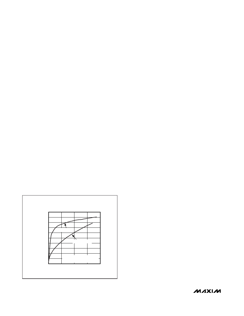
The theoretical best efficiency of a linear amplifier is
78%, however, that efficiency is only exhibited at peak
output power. Under normal operating levels (typical
music reproduction levels), efficiency falls below 30%,
whereas the MAX9877 still exhibits 70% efficiency
under the same conditions (Figure 3).
Ultra-Low EMI Filterless Output Stage
In traditional Class D amplifiers, the high dV/dt of the
rising and falling edge transitions results in increased
EMI emissions, which requires the use of external LC
filters or shielding to meet EN55022 electromagnetic-
interference (EMI) regulation standards. Limiting the
dV/dt normally results in decreased efficiency. Maxim’s
active emissions limiting circuitry actively limits the
dV/dt of the rising and falling edge transitions, provid-
ing reduced EMI emissions, while maintaining up to
87% efficiency.
In addition to active emission limiting, the MAX9877
features a patented spread-spectrum modulation mode
that flattens the wideband spectral components.
Proprietary techniques ensure that the cycle-to-cycle
variation of the switching period does not degrade
audio reproduction or efficiency (see the
Typical
Operating Characteristics
). Select spread-spectrum
modulation mode through the I
2
C interface (Table 6). In
spread-spectrum modulation mode, the switching fre-
quency varies randomly by ±60kHz around the center
frequency (1.176MHz). The effect is to reduce the peak
energy at harmonics of the switching frequency. Above
10MHz, the wideband spectrum looks like white noise
for EMI purposes (see Figure 4).
Speaker Current Limit
Most applications will not enter current limit unless the
output is short circuited or connected incorrectly.
When the output current of the speaker amplifier
exceeds the current limit (1.5A, typ) the MAX9877 dis-
ables the outputs for approximately 250µs. At the end of
250µs, the outputs are re-enabled, if the fault condition
still exists, the MAX9877 will continue to disable and re-
enable the outputs until the fault condition is removed.
Bypass Mode
The integrated DPST analog audio switch allows the
MAX9877’s Class D amplifier to be bypassed. In
bypass mode, the Class D amplifier is automatically
disabled allowing an external amplifier to drive the
speaker connected between OUT+ and OUT- through
RXIN+ and RXIN- (see the
Typical Application Circuit
).
The bypass switch is enabled at startup. The switch can
be opened or closed even when the MAX9877 is in soft-
ware shutdown (see the
I
2
C Register Description
section).
Unlike discrete solutions, the switch design reduces
coupling of Class D switching noise to the RXIN_
inputs. This eliminates the need for a costly T-switch.
The bypass switch is typically used with two 9.1
Ω resis-
tors connected to each input. These resistors, in combi-
nation with the switch on-resistance and an 8
Ω load,
approximate the 32
Ω load expected by the external
amplifier. Although not required, using the resistors
optimizes THD+N.
Drive RXIN+ and RXIN- with a low-impedance source
to minimize noise on the pins. In applications that do
not require the bypass mode, leave RXIN+ and RXIN-
unconnected.
MAX9877 EFFICIENCY
vs. IDEAL CLASS EFFICIENCY
MAX9877 fig03
OUTPUT POWER (W)
EFFICIENCY (%)
0.75
0.50
0.25
10
20
30
40
50
60
70
80
90
100
0
0
1.00
MAX9877
IDEAL CLASS AB
V
DD
= PV
DD
= 3.7V (MAX9877)
V
SUPPLY
= 3.7V (IDEAL CLASS AB)
Figure 3. MAX9877 Efficiency vs. Class AB Efficiency