verify algorithm, extra memory mapping – Rainbow Electronics T89C51RD2 User Manual
Page 68

Rev. F - 15 February, 2001
68
T89C51RD2
•
Step 8: Input the valid address on the address lines.
•
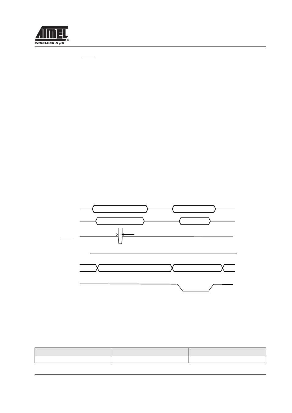
Step 9: Pulse ALE/PROG once until P3.2 is high or the specified write time is reached.
Repeat step 0 through 9 changing the address and data until the entire array or until the end of the object file is
reached (See Figure 23.)
•
Step 10: Disable programming access (PELCK mode)
8.9.5. Verify algorithm
Verify must be done after each byte or block of bytes is programmed. In either case, a complete verify of the
programmed array will ensure reliable programming of the T89C51RD2.
P 2.7 is used to enable data output.
To verify the T89C51RD2 code the following sequence must be exercised:
•
Step 1:Activate the combination of program and control signals (PGMV)
•
Step 2: Input the valid address on the address lines.
•
Step 3: Read data on the data lines.
Repeat step 2 through 3 changing the address for the entire array verification (See Figure 23.).
Figure 23. Programming and Verification Signal’s Waveform
8.9.6. Extra memory mapping
The memory mapping the T89C51RD2 software registers in the Extra FLASH memory is described in the table below.
Table 34. Extra Row Memory Mapping (XAF)
Address
Default content
Copy of device ID #3
0061h
FFh
Control signals
Data In
ALE/PROG
A0-A15
Programming Cycle
D0-D7
EA
Data Out
Read/Verify Cycle
5V
0V
P2.7
48 clk (load latch ) or 10 ms (write)
