Vishay semiconductors – C&H Technology 70MT060WSP User Manual
Page 4
70MT060WSP
www.vishay.com
Vishay Semiconductors
Revision: 07-Sep-11
3
Document Number: 93410
For technical questions within your region:
,
,
THIS DOCUMENT IS SUBJECT TO CHANGE WITHOUT NOTICE. THE PRODUCTS DESCRIBED HEREIN AND THIS DOCUMENT
ARE SUBJECT TO SPECIFIC DISCLAIMERS, SET FORTH AT
www.vishay.com/doc?91000
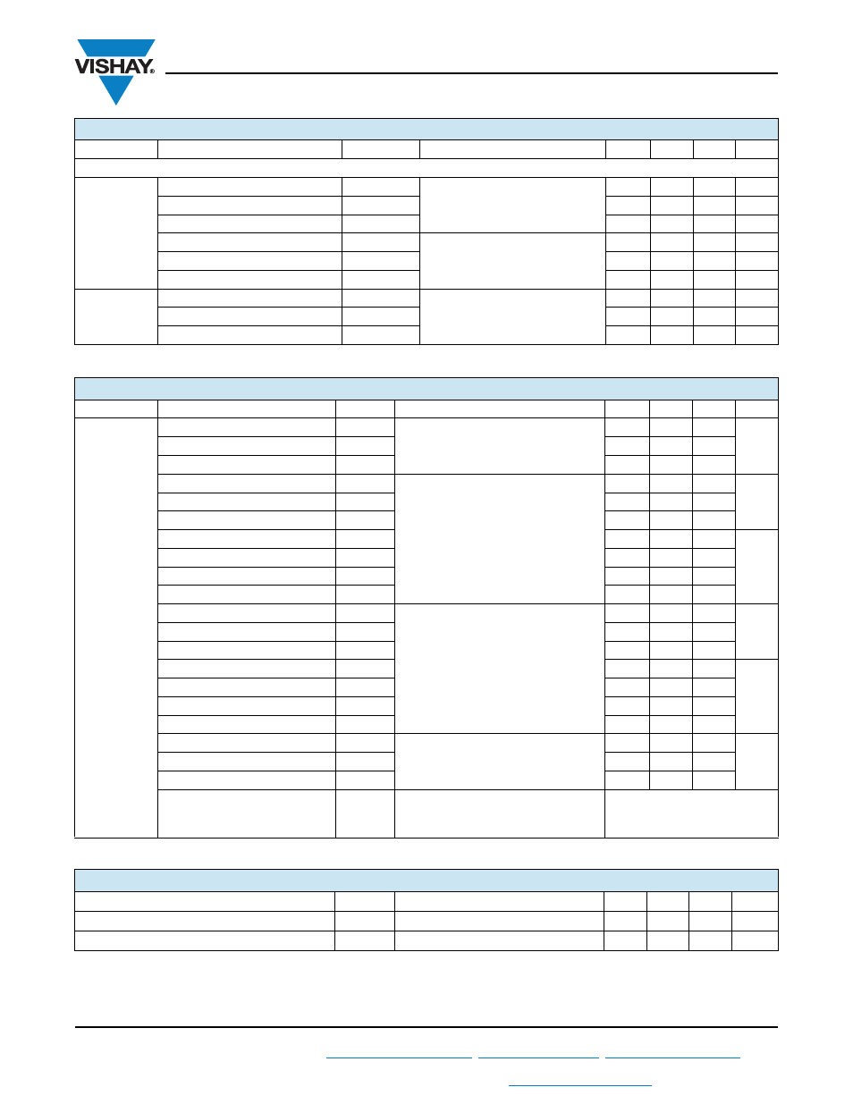
Notes
• Repetitive rating; pulsed with limited by maximum junction temperature.
RECOVERY PARAMETER
PFC Diode
Peak reverse recovery current
I
rr
I
F
= 40 A
dI/dt = 200 A/μs
V
R
= 200 V
-
4
7
A
Reverse recovery time
t
rr
-
59
79
ns
Reverse recovery charge
Q
rr
-
118
180
nC
Peak reverse recovery current
I
rr
I
F
= 40 A, T
J
= 125 °C
dI/dt = 200 A/μs
V
R
= 200 V
-
12
17
A
Reverse recovery time
t
rr
-
127
170
ns
Reverse recovery charge
Q
rr
-
733
1200
nC
AP Diode
Peak reverse recovery current
I
rr
I
F
= 4 A
dI/dt = 200 A/μs
V
R
= 200 V
-
7
10
A
Reverse recovery time
t
rr
-
78
120
ns
Reverse recovery charge
Q
rr
-
290
600
nC
SWITCHING CHARACTERISTICS (T
J
= 25 °C unless otherwise noted)
PARAMETER
SYMBOL
TEST CONDITIONS
MIN.
TYP.
MAX.
UNITS
PFC IGBT
Total gate charge
Q
g
I
C
= 50 A
V
CC
= 400 V
V
GE
= 15 V
-
320
-
nC
Gate to source charge
Q
gs
-
42
-
Gate to drain (Miller) charge
Q
gd
-
110
-
Turn-on switching loss
E
on
I
C
= 70 A, V
CC
= 360 V, V
GE
= 15 V
R
g
= 5
, L = 500 μH, T
J
= 25 °C
-
0.13
-
mJ
Turn-off switching loss
E
off
-
0.18
-
Total switching loss
E
tot
-
0.31
-
Turn-on delay time
t
d(on)
-
193
-
ns
Rise time
t
r
-
35
-
Turn-off delay time
t
d(off)
-
202
-
Fall time
t
f
-
49
-
Turn-on switching loss
E
on
I
C
= 70 A, V
CC
= 360 V, V
GE
= 15 V
R
g
= 5
, L = 500 μH, T
J
= 125 °C
-
0.25
-
mJ
Turn-off switching loss
E
off
-
0.32
-
Total switching loss
E
tot
-
0.57
-
Turn-on delay time
t
d(on)
-
193
-
ns
Rise time
t
r
-
35
-
Turn-off delay time
t
d(off)
-
208
-
Fall time
t
f
-
66
-
Input capacitance
C
ies
V
GE
= 0 V
V
CC
= 30 V
f = 1 MHz
-
7430
-
pF
Output capacitance
C
oes
-
530
-
Reverse transfer capacitance
C
res
-
94
-
Reverse bias safe operating area
RBSOA
I
C
= 250 A, V
CC
= 400 V, V
P
= 600 V,
R
g
= 22
, V
GE
= 15 V, L = 500 μH,
T
J
= 150 °C
Full square
THERMISTOR ELECTRICAL CHARACTERISTICS (T
J
= 25 °C unless otherwise noted)
PARAMETER
SYMBOL
TEST CONDITIONS
MIN.
TYP. MAX. UNITS
Resistance
R
T
J
= 25 °C
-
30 000
-
B value
B
T
J
= 25 °C/T
J
= 85 °C
-
4000
-
K
ELECTRICAL SPECIFICATIONS (T
J
= 25 °C unless otherwise noted)
PARAMETER
SYMBOL
TEST CONDITIONS
MIN.
TYP.
MAX.
UNITS