Vishay semiconductors – C&H Technology 70MT060WSP User Manual
Page 10
70MT060WSP
www.vishay.com
Vishay Semiconductors
Revision: 07-Sep-11
9
Document Number: 93410
For technical questions within your region:
,
,
THIS DOCUMENT IS SUBJECT TO CHANGE WITHOUT NOTICE. THE PRODUCTS DESCRIBED HEREIN AND THIS DOCUMENT
ARE SUBJECT TO SPECIFIC DISCLAIMERS, SET FORTH AT
www.vishay.com/doc?91000
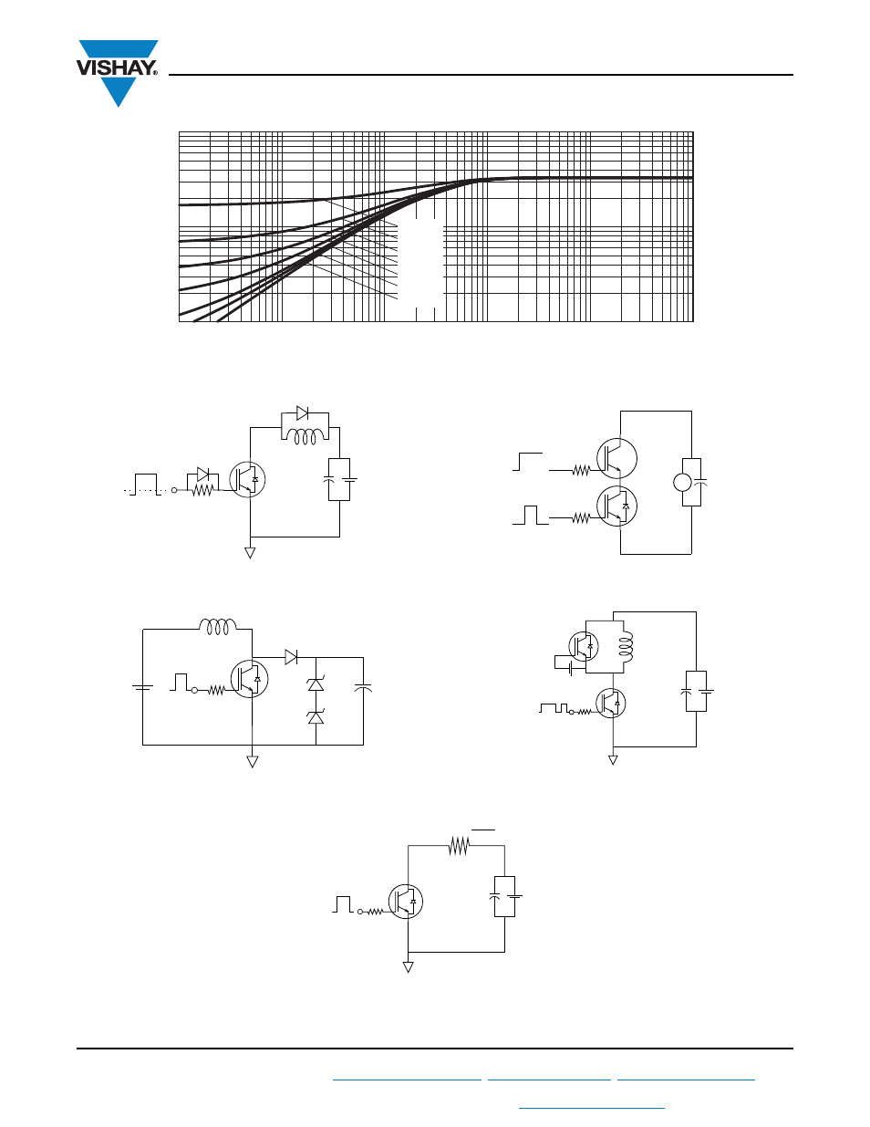
Fig. 28 - Maximum Thermal Impedance Z
thJC
Characteristics (IGBT)
Fig. C.T.1 - Gate Charge Circuit (Turn-Off)
Fig. C.T.2 - RBSOA Circuit
Fig. C.T.3 - S.C. SOA Circuit
Fig. C.T.4 - Switching Loss Circuit
Fig. C.T.5 - Resistive Load Circuit
0.01
0.1
1
0.0001
93410_28
0.001
0.01
0.1
1
t
1
- Rectangular Pulse Duration (s)
Z
thJC
- Transient Thermal Impe
d
ance
Junction to Case (°C/W)
10
D = 0.50
D = 0.20
D = 0.10
D = 0.05
D = 0.02
D = 0.01
DC
1K
V
CC
D.U.T.
0
L
+
-
L
80 V
R
g
1000 V
D.U.T.
+
-
Driver
D.U.T.
900 V
D
C
+
-
L
Diode clamp/
D.U.T.
D.U.T./
Driver
- 5 V
+
-
R
g
V
CC
+
-
R
g
D.U.T.
R =
V
CC
I
CM
V
CC
+
-
- TDK4_ _3302 (5 pages)
- CM75TL-12NF (5 pages)
- PM600HSA120 (5 pages)
- GLI......A (4 pages)
- PM600DVA060 (5 pages)
- VSKDS408-060 (10 pages)
- G200 (5 pages)
- VS30ASR..N Series (2 pages)
- LPS1100 (6 pages)
- PM50CL1B120 (6 pages)
- CPS (3 pages)
- PM200DSA060 (7 pages)
- RM400HA-34S (5 pages)
- VS-GB100TH120U (8 pages)
- PP300B120 (8 pages)
- PP400B060 (8 pages)
- PM100RLA060 (7 pages)
- PM25RL1A120 (8 pages)
- VS210DG..HCB Series (3 pages)
- RTO20 (5 pages)
- PM50B4LB060 (7 pages)
- VS-GT100DA120U (11 pages)
- PM200RLA060 (7 pages)
- ST380CHPbF Series (8 pages)
- RM1200DB-66S (11 pages)
- GB70NA60UF (6 pages)
- VS255SG..HCB Series (3 pages)
- EMF050J60U (18 pages)
- HFA30TA60CSPbF (6 pages)
- PM50CLB120 (5 pages)
- MBR10.. Series (7 pages)
- VS-GB300LH120N (7 pages)
- LTO100 (5 pages)
- ST303CLPbF Series (9 pages)
- PM100CVA060 (7 pages)
- ST230CPbF Series (8 pages)
- QR_1220T30 (5 pages)
- VS230LM06CS02CB (3 pages)
- ST303CPbF Series (9 pages)
- TDK4_ _3002 (5 pages)
- HFA240NJ40CPbF (8 pages)
- CT220802 (5 pages)
- VS-UFL130FA60 (8 pages)
- GB05XP120KTPbF (11 pages)
- VS-GT75NP120N (7 pages)