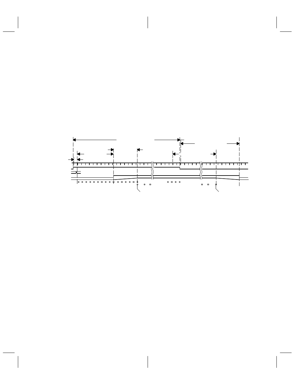
Figure 4–1. power ramp-up/ramp-down timing diagram – Texas Instruments TCM4300 User Manual
Page 41

4–6
delay after the last symbol occurs (2 SINT periods before TXGO goes low); then the transmit outputs decay
to zero differential voltage (each output at the voltage supplied to the VCM input terminal). The shape of the
decay is the transient resulting from the internal SQRC filtering. The transmit outputs are held at zero
differential voltage 6 SINT periods (3 symbol periods) after the start of the decay. At this time the PAEN digital
output is set low (see Figure 4–1 and Figure 4–2).
Nonzero values of the BST offset register increase the delays of both the transmit waveforms and PAEN
relative to the edges of TXGO after it is internally sampled by SINT. The delays are increased in increments
of 1/4 SINT (1/8 symbol period).
For delays of 1 SINT or greater, the fractional part of the delay can be achieved using the BST offset register
with the remaining integer SINT delay implemented externally by delaying the writing to TXGO and TXI.
The relative timing of PAEN and the transmit waveforms is not affected by the BST offset register.
The IS-54 standard describes shortened bursts and normal bursts. The two types differ in duration and
number of transmitted bursts, burst length being determined by the TXGO bit.
First MEP
Last MEP
>>>
>>>
>>>
SINT
TXGO
TXI data bit
PAEN
TXI/Q output ramp
Input Bits
Dibit transmission
† Total delay = d (SINT/4 or T/8) where d = integer value (0,1,2,3) written to the BST offset register.
6 SINT Periods
d(T/8)
†
9.5 SINT Periods
N+3 SINT Periods
(N = Total number of bits sent)
15.5 SINT Periods +d(T/8)
>>>
19.5 SINT Periods +d(T/8)
Figure 4–1. Power Ramp-Up/Ramp-Down TIming Diagram
