Texas Instruments TCM4300 User Manual
Page 39

4–4
square-root raised-cosine (SQRC) shaping filter with a roll-off rate of
α
= 0.35 and converted to sampled
analog form by two 9-bit digital-to-analog converters (DACs). The output of the DAC is then filtered by a
continuous-time resistance-capacitance (RC) filter.
The TCM4300 generates a power amplifier (PA) control signal, PAEN, to enable the power supply for the
PA. The start and stop times of the TDM burst are controlled by writing to a single bit, TXGO, in the DSP
DStatCtrl register.
In the analog mode (MODE = 0), the DSP writes 8-bit I and Q samples into the TXI and TXQ data registers
at a 40-ksps rate. These writes are timed by the SINT interrupt signal. The samples are fed to a low-pass
filter before D / A conversion. In the transmit analog mode, PAEN is always set to 1.
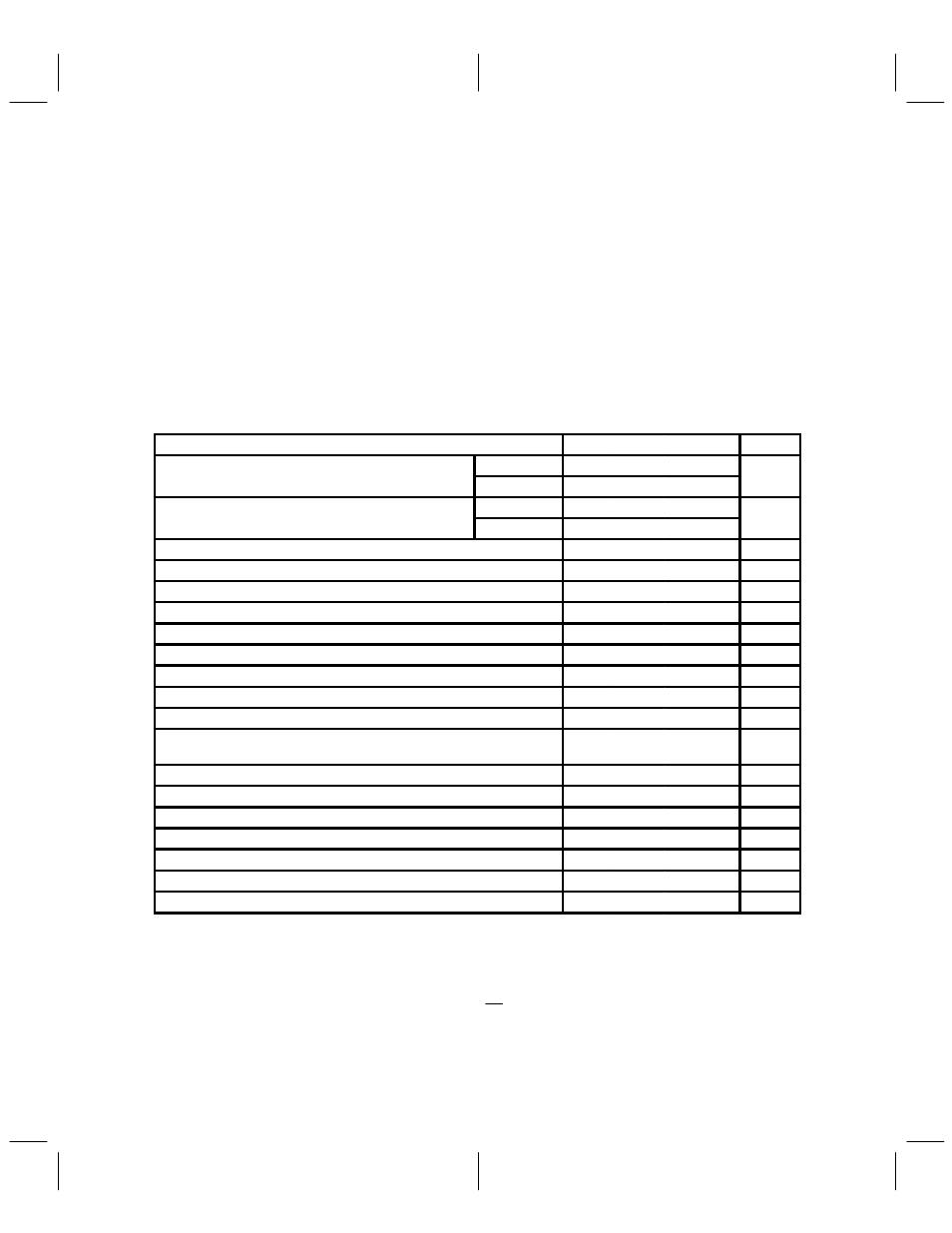
The transmit section provides differential I and Q outputs (see Table 4-5) for both analog and digital modes.
The differential dc offset for the TXI and TXQ outputs can be independently adjusted using the transmit offset
registers.
Table 4–5. Transmit (TX) I and Q Channel Outputs
PARAMETER
MIN
TYP
MAX
UNIT
Peak output voltage full scale centered at VCM
Differential
2.24
Vp
Peak output voltage full scale, centered at VCM
Single ended
1.12
Vp
Nominal output-level (constellation radius) centered at
Differential
1.5
V
Nominal output level (constellation radius) centered at
VCM
Single ended
0.75
V
Low-level drift
±
200
PPM/
°
C
Transmit error vector magnitude (EVM)
3%
4%
Resolution
8
bits
S/(N+D) ratio at differential outputs
48
52
dB
Gain error (I or Q channel)
±
8%
±
12%
Gain mismatch between I and Q
±
0.3
dB
Gain sampling mismatch between I and Q
20
ns
Zero code error differential
±
80
mV
Zero code error, each output, with respect to VCM
±
80
mV
Zero code error, I to Q, with respect to other channel (differential or
single ended)
±
10
mV
Load impedance, between P and N terminals
10
k
Ω
Transmit offset DACs I and Q resolution
6
bits
Transmit offset DACs I and Q average step size
2.9
3.4
3.9
mV
Transmit offset DACs I and Q full-scale positive output
105.4
mV
Transmit offset DACs I and Q full-scale negative output
– 108.8
mV
Transmit offset DACs differential nonlinearity
±
1.1
LSB
Transmit offset DACs integral nonlinearity
±
1.1
LSB
Modulation Error: In the digital mode, during the transmit burst, the complex output of the transmitter circuits
consists of an ideal output s = I
ideal
+ jQ
ideal
+ error e = e
i
+ je
q
. In Table 4-5, the modulation error vector
magnitude (EVM) is defined as the peak value of the magnitude of e relative to the ideal output:
Modulation error percentage
+
100
|e|
|s|
%
Table 4–6 and Table 4–7 show the frequency response of the transmit section for digital and analog mode,
respectively.
