Texas Instruments TCM4300 User Manual
Page 25
3–2
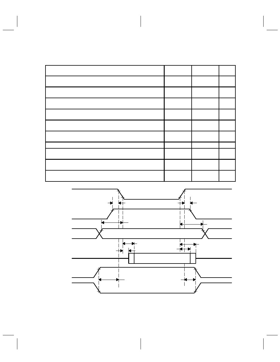
3.2
TCM4300 to Microcontroller Interface Timing Requirements (Mitsubishi
Read Cycle) (see Figure 3–2 and Note 2)
PARAMETER
ALTERNATE
SYMBOL
MIN
MAX
UNIT
tsu(R/W)
Setup time, read/write MCRW stable before falling edge of
strobe MCDS
TRW(SU)
0
ns
th(R/W)
Hold time, read/write MCRW stable after rising edge of
strobe MCDS
TRW(HO)
10
ns
tsu(RA)
Setup time, read address MCS stable before falling edge of
strobe MCDS
TRA(SU)
0
ns
th(RA)
Hold time, read address MCA stable after rising edge of
strobe MCDS
TRA(HO)
10
ns
ten(RD)
Enable time, read data on falling edge of strobe MCDS to
TCM4300 driving data bus MCD
TRD(EN)
10
ns
tv(R)
Read data valid time on falling edge of strobe MCDS to
valid data MCD
TRD(DV)
50
ns
tinv
Data MCD invalid after rising edge of strobe MCDS
TRD(INV)
10
ns
tdis(RD)
Disable time, read data. TCM4300 releases MCD data bus
after rising edge of strobe MCDS
TRD(DIS)
28
ns
th(CS)
Hold time, chip select MCCSH and MCCSL stable before
rising edge of strobe MCDS
TCS(HO)
0
ns
tsu(CS)
Setup time, chip select MCCSH and MCCSL stable before
falling edge of strobe MCDS
TCS(SU)
0
ns
NOTE 2: Timings are based upon Mitsubishi 37732S4 (16 MHz) and Mitsubishi 3772S4L (8 MHz).
MCA4–MCA0
MCD7–MCD0
MCDS
(see Note A)
MCRW
ОО
ОО
О
О
10%
90%
90%
10%
90%
90%
tsu(R / W)
tv(R)
ten(RD)
tdis(RD)
tinv
tsu(CS)
th(CS)
MCCSH
MCCSL
90%
90%
10%
10%
NOTE A: Chip selection is defined as both MCCS and MCDS active.
th(R / W)
tsu(RA)
th(RA)
Figure 3–2. Microcontroller Interface Timing Requirements
(Mitsubishi Configuration Read Cycle, MTS [1:0] = 10)