4 watchdog timer, 5 port i/o timing – Renesas M34502T-MCU User Manual
Page 28
( 26 / 38 )
Figure 5.1 Waveform output from check pin TP5
5.5 Port I/O Timing
(1) Port input timing
Port input timings are the same as with each actual MCU.
(2) Port output timing
The output timings of the following ports are different from those of actual MCUs because of the
emulation circuits configured with the ports of the M34502T-MCU.
• Ports D
0
to D
5
• Ports P0
0
to P0
3
• Ports P1
0
to P1
3
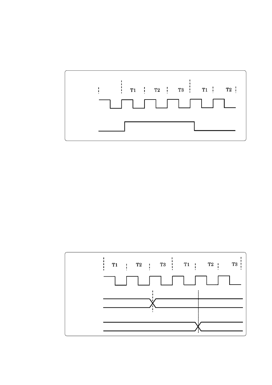
With actual MCUs, the changes occur at the beginning of the T3 state of an output instruction,
while with the M34502T-MCU, the changes occur at the beginning of the T2 state of the next
output instruction. Figure 5.2 shows the port output timings of actual MCUs and the M34502T-
MCU. For the other ports, the output timings are the same as those of actual MCUs.
5.4 Watchdog Timer
The M34502T-MCU does not have an operational watchdog timer. Therefore, use an evaluation
MCU (OTP version) to verify the operation associated with a watchdog timer.
The M34502T-MCU outputs a signal whose waveform is shown below from the check pin TP5
during WRST instruction execution cycles. This signal allows you to check the initialization cycle
of a watchdog timer.
Figure 5.2 D, P0 and P1 port output timings
Next output instruction
Output instruction
System clock
X
IN
P0, P1, D port
output timings
on actual MCUs
P0, P1, D port
output timings of
M34502T-MCU
WRST instruction
Next instruction
System clock
X
IN
WRST