Renesas M34502T-MCU User Manual
Page 24
( 22 / 38 )
Table 4.9 M34501T-PTC pin assignments
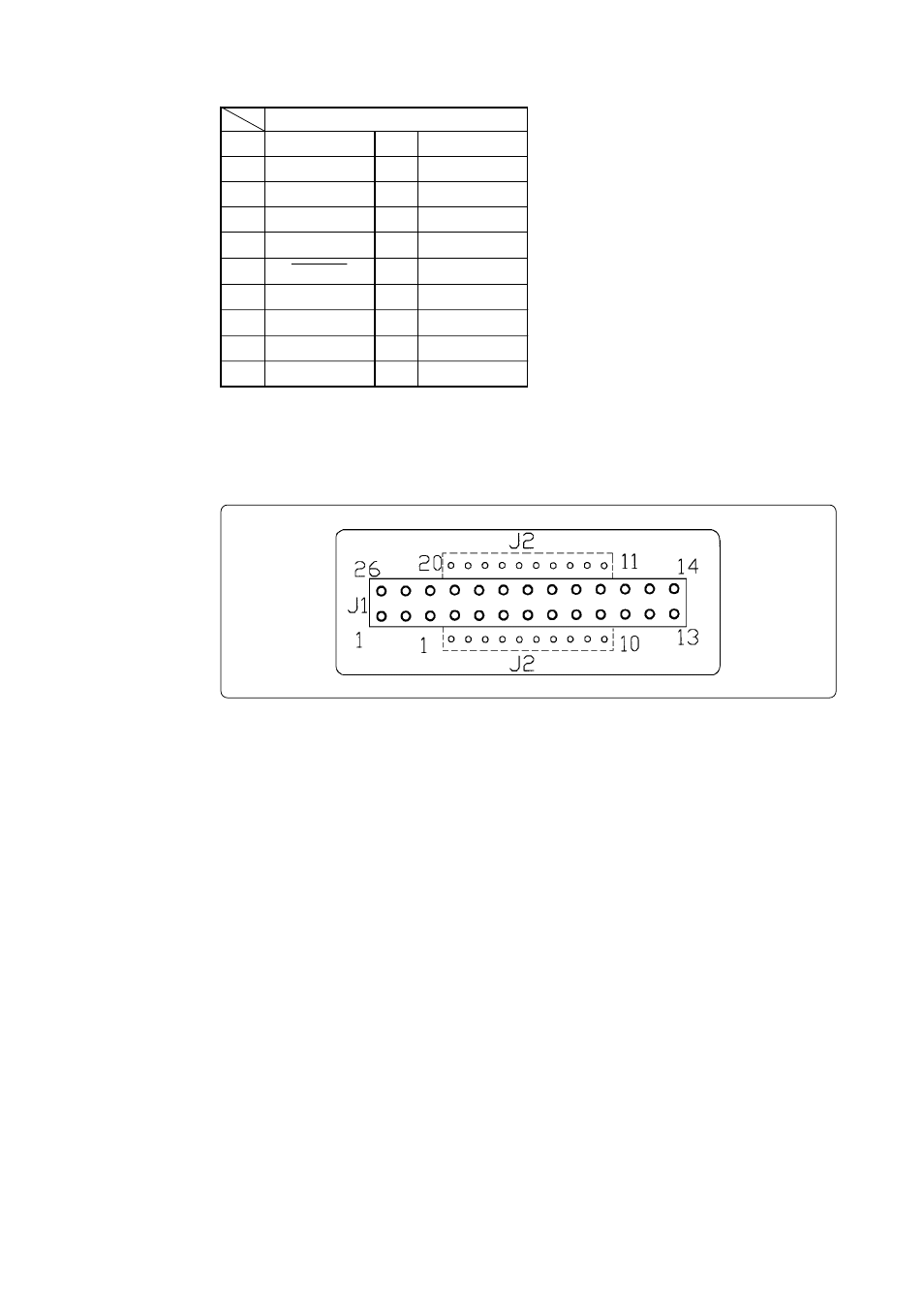
Figure 4.11 Pin layout of the M34501T-PTC
*1 EV
DD
does not input the power supply from the target system, but outputs it to the target system
from the power circuit on the M34502T-MCU.
*2 X
IN
is input from oscillator circuit board OSC-2 on the M34502T-MCU and cannot be input from
the oscillator circuit on the target system.
1
2
3
4
5
6
7
8
9
10
EV
DD
*
1
V
SS
NC (X
IN
*
2
)
NC (X
OUT
)
NC (CNV
SS
)
ERESET
EP2
1
/A
IN1
EP2
0
/A
IN0
ED
3
ED
2
20
19
18
17
16
15
14
13
12
11
EP0
0
EP0
1
EP0
2
EP0
3
EP1
0
EP1
1
EP1
2
/CNTR
EP1
3
/INT
ED
0
ED
1
M34501T-PTC J2
See also other documents in the category Renesas Hardware:
- Single-Chip Microcomputer M34551T2-MCU (42 pages)
- M3T-FLX-80NRA (6 pages)
- 70 (162 pages)
- M16C/30P (102 pages)
- PROM Programming Adapter PCA7427G02 (20 pages)
- R0E572110CFK00 (40 pages)
- H8/325 Series (20 pages)
- Single-Chip Microcomputer H8/36079 (27 pages)
- Direct Dummy IC M3T-DIRECT100S (4 pages)
- M3A-2152 (95 pages)
- PCA7755D (6 pages)
- M16C/6N5 (106 pages)
- SH7085 (50 pages)
- QFP-144 (23 pages)
- H8/3834 Series (22 pages)
- RSKM16C62P (3 pages)
- H8/33937 (22 pages)
- Single-Chip Microcomputer H8SX/1622 (5 pages)
- E6000 (29 pages)
- PCA7400 (18 pages)
- PCA4738FF-64 (20 pages)
- SuperH HS7339KCU01HE (43 pages)
- M16C FAMILY (103 pages)
- PCA7412F-100 (20 pages)
- 4513 (210 pages)
- M34551E8FP (16 pages)
- Dummy IC M3T-SSOP36B-450 (4 pages)
- Emulation Pod M30100T3-RPD-E (52 pages)
- Converter Board for M30102 M30102T-PTC (4 pages)
- SH7145 (31 pages)
- HS1653ECN61H (36 pages)
- Converter Board R0E521276CFG00 (4 pages)
- PCA7302E1F-80 (18 pages)
- H8/3814 Series (21 pages)
- H8S/2646 Series (20 pages)
- SuperHTM Family SH7125 Series (40 pages)
- M30262T-PTC (4 pages)
- SH7670 (82 pages)
- H8/3864 Series (20 pages)
- Emulator System M3T-MR100 (306 pages)
- 38K0 (6 pages)
- PLQP0176KB-A (40 pages)
- Direct Dummy IC M3T-DIRECT80S (6 pages)
- PCA4738L-80A (26 pages)
- Converter Board R0E5212BACFG00 (6 pages)