Ni vxipc-882 functional block diagram, Figure 1-1. ni vxipc-882 block diagram, Ni vxipc-882 functional description – National Instruments NI VXIpc-882 User Manual
Page 12
Chapter 1
Introduction
1-2
ni.com
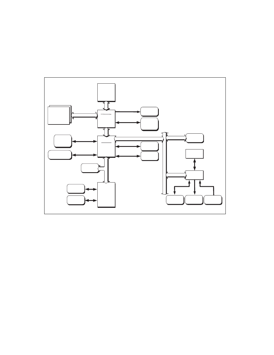
NI VXIpc-882 Functional Block Diagram
Figure 1-1 is a functional block diagram of the NI VXIpc-882 controller.
Figure 1-1. NI VXIpc-882 Block Diagram
NI VXIpc-882 Functional Description
This section contains brief functional descriptions of the major
NI VXIpc-882 logic blocks shown in Figure 1-1.
•
The SO-DIMM block consists of two DDR2 SDRAM sockets that can
hold up to 2 GB each.
•
The Gigabit Ethernet connects to either 10 Mbit, 100 Mbit, or
1,000 Mbit Ethernet interfaces.
•
The Watchdog Timer block consists of a watchdog timer that can reset
the controller.
Intel Core 2
Duo CPU
Graphics
Memory
Controller
Hub
DVI-I
Connector
Gigabit
Ethernet
I/O
Controller
Hub
LPT
COM 1
Watchdog
Super I/O
LPC Bus
DMI
Chip Set
Chip Set
VXI
Interface
External
Clock SMB
VXI Trigger
IN SMB
VXI Trigger
OUT SMB
GPIB
PCI Bus
DUAL CH
Hard Drive
Flash ROM
ExpressCard/34
Slot
4 Hi-Speed
USB Ports
2 SO-DIMMs
DDR2 SDRAM
PC2 5300
Trigger
Card