Philips SC28L91 User Manual
Page 21
Philips Semiconductors
Product data sheet
SC28L91
3.3 V or 5.0 V Universal Asynchronous
Receiver/Transmitter (UART)
2004 Oct 21
21
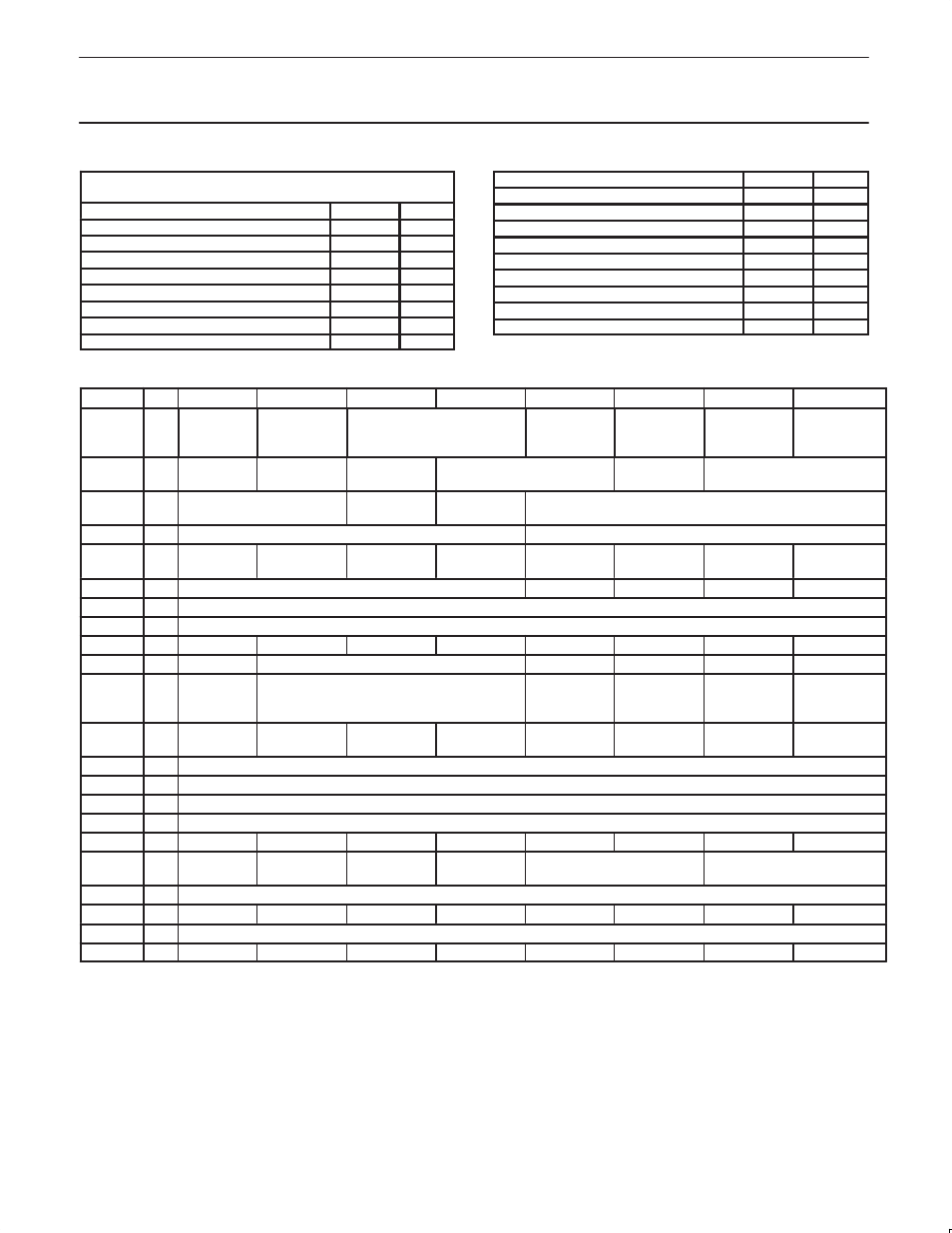
Register Acronyms and Read / Write Capability
(R/W = Read/Write, R = Read only, W = Write only)
Mode Register
MRn
R/W
Status Register
SR
R
Clock Select
CSR
W
Command Register
CR
W
Receiver FIFO
RxFIFO
R
Transmitter FIFO
RxFIFO
W
Input Port Change Register
IPCR
R
Auxiliary Control Register
ACR
W
Interrupt Status Register
ISR
R
Interrupt Mask Register
IMR
W
Counter Timer Upper Value
CTU
R
Counter Timer Lower Value
CTL
R
Counter Timer Preset Upper
CTPU
W
Counter Timer Preset Lower
CTPL
W
Input Port Register
IPR
R
Output Configuration Register
OPCR
W
Set Output Port
Bits
W
Reset Output Port
Bits
W
Interrupt vector or GP register
IVR/GP
R/W
Table 2. Condensed Register bit formats
N
ame
Adr
Bit 7
Bit 6
Bit 5
Bit 4
Bit 3
Bit 2
Bit 1
Bit 0
MR0
0
WATCH
DOG
RxINT BIT 2
TxINT [1:0]
FIFO SIZE
BAUD RATE
EXTENDED
II
TEST 2
BAUD RATE
EXTENDED 1
MR1
0
RxRTS
Control
RxINT BIT 1
Error Mode
Parity Mode
Parity Type
Bits per Character
MR2
0
Channel Mode
TxRTS
Control
CTSN Enable
Tx
Stop Bit Length
CSR
1
Receiver Clock, Select Code
Transmitter Clock select code,
SR
1
Received
Break
Framing
Error
Parity Error
Overrun Error
TxEMT
TxRDY
RxFULL
RxRDY
CR
2
Channel Command codes
Disable Tx
Enable Tx
Disable Rx
Enable Rx
RxFIFO
3
Read 8 bits from Rx FIFO
TxFIFO
3
Write 8 bits to Tx FIFO
IPCR
4
Delta IP3
Delta IP2
Delta IP1
Delta IP0
State of IP3
State of IP2
State of IP1
State of IP0
ACR
4
Baud Group
Counter Timer mode and clock select
Enable IP3
Enable IP2
Enable IP1
Enable IP0
ISR
5
Change
Input Port
Ignore in ISR Reads
Counter
Ready
Change
Break
RxRDY
TxRDY
IMR
5
Change
Input Port
Set to 0
Set to 0
Set to 0
Counter
Ready
Change
Break
RxRDY
TxRDY
CTU
6
Read 8 MSb of the BRG Timer divisor.
CTPU
6
Write 8 MSb of the BRG Timer divisor.
CTL
7
Read 8 LSb of the BRG Timer divisor.
CTPL
7
Write 8 LSb of the BRG Timer divisor.
IPR
D
State of IP
State of IP 6
State of IP 5
State of IP 4
State of IP 3
State of IP 2
State of IP1
State of IP 0
OPCR
D
Configure
OP7
Configure
OP6
Configure
OP5
Configure
OP4
Configure OP3
Configure OP2
Strt C/T
E
Read Address E to start Counter Timer
SOPR
E
Set OP 7
Set OP 6
Set OP 5
Set OP 4
Set OP 3
Set OP 2
Set OP 1
Set OP 0
Stp C/T
F
Read Address F to stop counter Timer
ROPR
F
Reset OP 7
Reset OP 6
Reset OP 5
Reset OP 4
Reset OP 3
Reset OP 2
Reset OP 1
Reset OP 0