Pinning information, 1 pinning, 2 pin description – Philips TDA5051A User Manual
Page 4: Tda5051a, Nxp semiconductors
TDA5051A
All information provided in this document is subject to legal disclaimers.
© NXP B.V. 2011. All rights reserved.
Product data sheet
Rev. 5 — 13 January 2011
4 of 29
NXP Semiconductors
TDA5051A
Home automation modem
7. Pinning
information
7.1 Pinning
7.2 Pin description
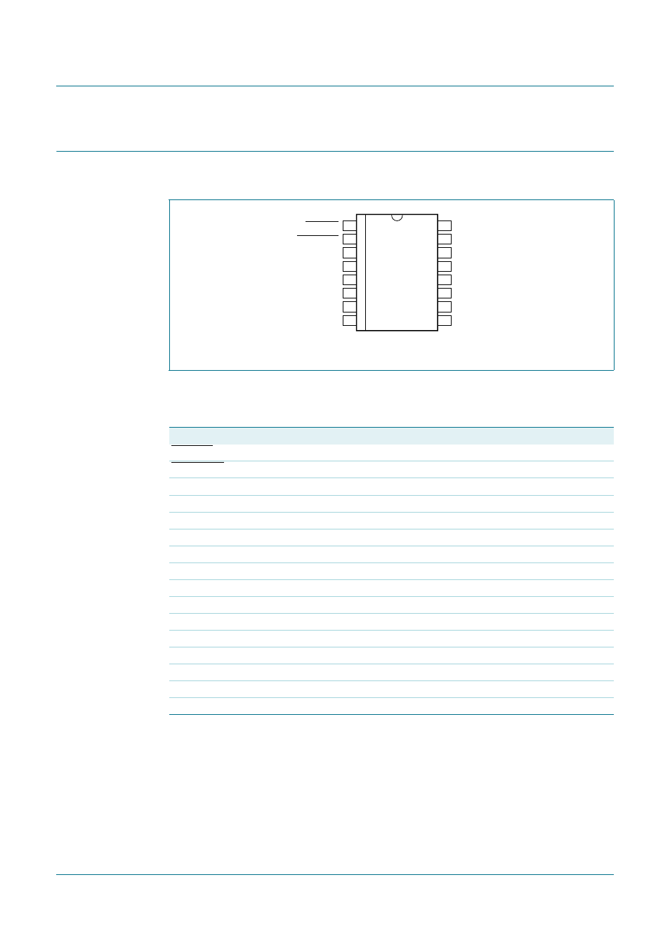
Fig 2.
Pin configuration for SO16
TDA5051AT
DATA_IN
TEST1
DATA_OUT
PD
V
DDD
RX_IN
CLK_OUT
V
DDA
DGND
AGND
SCANTEST
V
DDAP
OSC1
TX_OUT
OSC2
APGND
002aaf039
1
2
3
4
5
6
7
8
10
9
12
11
14
13
16
15
Table 3.
Pin description
Symbol
Pin
Description
DATA_IN
1
digital data input (active LOW)
DATA_OUT
2
digital data output (active LOW)
V
DDD
3
digital supply voltage
CLK_OUT
4
clock output
DGND
5
digital ground
SCANTEST
6
test input (LOW in application)
OSC1
7
oscillator input
OSC2
8
oscillator output
APGND
9
analog ground for power amplifier
TX_OUT
10
analog signal output
V
DDAP
11
analog supply voltage for power amplifier
AGND
12
analog ground
V
DDA
13
analog supply voltage
RX_IN
14
analog signal input
PD
15
power-down input (active HIGH)
TEST1
16
test input (HIGH in application)