Timing, 1 configuration for clock, Figure 6 – Philips TDA5051A User Manual
Page 11: Figure 7, Tda5051a, Nxp semiconductors
TDA5051A
All information provided in this document is subject to legal disclaimers.
© NXP B.V. 2011. All rights reserved.
Product data sheet
Rev. 5 — 13 January 2011
11 of 29
NXP Semiconductors
TDA5051A
Home automation modem
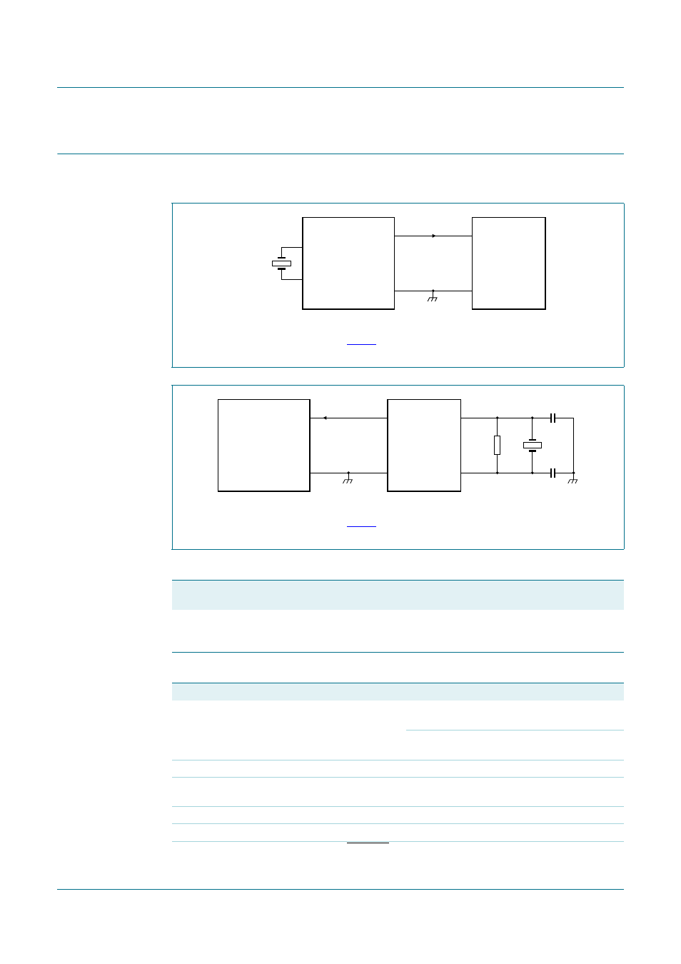
11. Timing
11.1 Configuration for clock
For parameter description, see
.
Fig 6.
External clock
For parameter description, see
.
Fig 7.
Typical configuration for on-chip clock circuit
Table 6.
Clock oscillator parameters
Oscillator
frequency f
osc
Carrier
frequency f
cr
Clock output frequency
1
⁄
2
f
osc
External components
6.080 MHz to
9.504 MHz
95 kHz to
148.5 kHz
3.040 MHz to 4.752 MHz
C1 = C2 = 27 pF to 47 pF;
R
p
= 2.2 M
Ω to 4.7 MΩ;
XTAL = standard quartz crystal
Table 7.
Calculation of parameters depending on the clock frequency
Symbol
Parameter
Conditions
Unit
f
osc
oscillator frequency
with on-chip oscillator: frequency of
the crystal quartz
Hz
with external clock: frequency of the
signal applied at OSC1
Hz
f
CLKOUT
clock output frequency
1
⁄
2
f
osc
Hz
f
cr
carrier frequency/digital filter tuning
frequency
1
⁄
64
f
osc
Hz
t
su
set-up time of the shaped burst
23/f
cr
or 1472/f
osc
s
t
h
hold time of the shaped burst
23/f
cr
or 1472/f
osc
s
t
W(DI)(min)
minimum pulse width of DATA_IN
signal
t
su
+ 1/f
cr
s
002aaf042
TDA5051A
7
5
OSC1
DGND
f
osc
CLK_OUT
GND
MICROCONTROLLER
XTAL
002aaf043
TDA5051A
4
5
CLK_OUT
DGND
1
/
2
f
osc
CLK_OUT
GND
MICROCONTROLLER
8
7
OSC2
OSC1
Rp
XTAL
C1
C2