Table 3.8 pll pins, Table 3.9 core and i/o power and ground pins, Pll pins – SMSC LAN9312 User Manual
Page 34: Core and i/o power and ground pins, Note 3.7, Datasheet
High Performance Two Port 10/100 Managed Ethernet Switch with 32-Bit Non-PCI CPU Interface
Datasheet
Revision 1.4 (08-19-08)
34
SMSC LAN9312
DATASHEET
Note 3.7
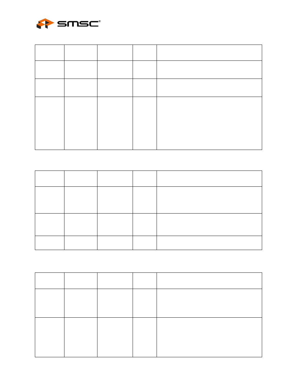
The input buffers are enabled when configured as GPIO inputs only.
75
Test 1
TEST1
AI
Test 1: This pin must be tied to VDD33IO for
proper operation.
108
Test 2
TEST2
AI
Test 2: This pin must be tied to VDD33IO for
proper operation.
62
Power
Management
Event
PME
O8/OD8
Power Management Event: When programmed
accordingly, this signal is asserted upon detection
of a wakeup event. The polarity and buffer type of
this signal is programmable via the PME_EN bit of
the
Power Management Control Register
Chapter 4, "Clocking, Resets, and Power
for additional
information on the LAN9312 power management
features.
Table 3.8 PLL Pins
PIN
NAME
SYMBOL
BUFFER
TYPE
DESCRIPTION
107
PLL +1.8V
Power Supply
VDD18PLL
P
PLL +1.8V Power Supply: This pin must be
connected to VDD18CORE for proper operation.
Refer to the LAN9312 application note for
additional connection information.
105
Crystal Input
XI
ICLK
Crystal Input: External 25MHz crystal input. This
signal can also be driven by a single-ended clock
oscillator. When this method is used, XO should be
left unconnected.
106
Crystal
Output
XO
OCLK
Crystal Output: External 25MHz crystal output.
Table 3.9 Core and I/O Power and Ground Pins
PIN
NAME
SYMBOL
BUFFER
TYPE
DESCRIPTION
7,13,21,27,
33,39,46,
54,64,66,
72,73,81,
87,93,100
+3.3V I/O
Power
VDD33IO
P
+3.3V Power Supply for I/O Pins and Internal
Regulator
Refer to the LAN9312 application note for
additional connection information.
3,14,40,65,
74,88,104
Digital Core
+1.8V Power
Supply
Output
VDD18CORE
P
Digital Core +1.8V Power Supply Output: +1.8V
power from the internal core voltage regulator. All
VDD18CORE pins must be tied together for proper
operation.
Refer to the LAN9312 application note for
additional connection information.
Table 3.7 Miscellaneous Pins (continued)
PIN
NAME
SYMBOL
BUFFER
TYPE
DESCRIPTION