2 data memory, 1 data memory addressing, Index register ix – Epson 6200A User Manual
Page 14
8
EPSON
S1C6200/6200A CORE CPU MANUAL
2 MEMORY AND OPERATIONS
2.2 Data Memory
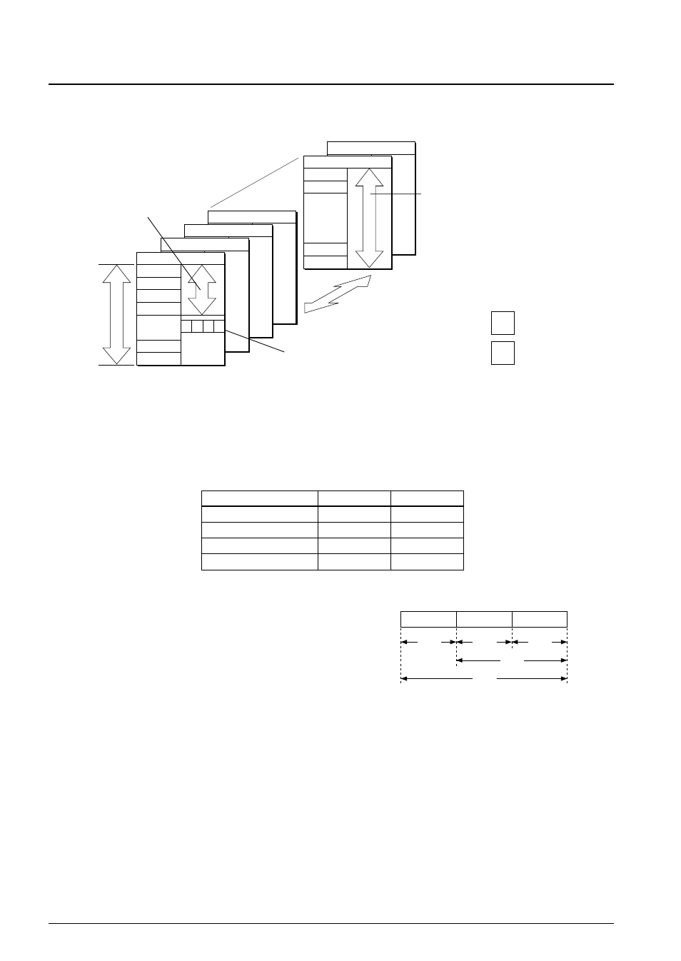
The data memory area comprises 4,096 4-bit words. The RAM, timer, I/O and other peripheral circuits are
mapped into this memory according to the designer's specifications. Figure 2.2.1 shows the data memory
configuration.
;;;;;;;
;;;;;;;
;;;;;;;
;;;;;;;
;;;;;;;
;;;;;;;
;;;;;;;
;;;;;;;
;;;;;;;
;;;;;;;
;;;;;;;
;;;;;;;
;;;;;;;
;;;;;;;
Page 15
;;;;;;;
;;;;;;;
;;;;;;;
;;;;;;;
;;;;;;;
;;;;;;;
;;;;;;;
;;;;;;;
;;;;;;;
;;;;;;;
;;;;;;;
;;;;;;;
;;;;;;;
;;;;;;;
Page 14
Step 0
Step 1
Step 254
Step 255
;;;;;;;
;;;;;;;
;;;;;;;
;;;;;;;
;;;;;;;
;;;;;;;
;;;;;;;
;;;;;;;
;;;;;;;
;;;;;;;
;;;;;;;
;;;;;;;
;;;;;;;
;;;;;;;
Page 3
;;;;;;;
;;;;;;;
;;;;;;;
;;;;;;;
;;;;;;;
;;;;;;;
;;;;;;;
;;;;;;;
;;;;;;;
;;;;;;;
;;;;;;;
;;;;;;;
;;;;;;;
;;;;;;;
Page 2
;;;;;;;
;;;;;;;
;;;;;;;
;;;;;;;
;;;;;;;
;;;;;;;
;;;;;;;
;;;;;;;
;;;;;;;
;;;;;;;
;;;;;;;
;;;;;;;
;;;;;;;
;;;;;;;
Page 1
;;;;;;;
;;;;;;;
;;;;;;;
;;;;;;;
;;;;;;;
;;;;;;;
;;;;;;;
;;;;;;;
;;;;;;;
;;;;;;;
;;;;;;;
;;;;;;;
;;;;;;;
;;;;;;;
;;;;;;;
Page 0
Step 0
Step 1
Step 15
Step 254
Step 255
;;;;
;;;;
;;;;
;;;;
;;;;
;;;;
;;;;
;;;;
XHL or YHL
(within page)
4-bit data
Memory or I/O
Register area
XP or YP
(page specification)
SP
Page 0
only
RP
Page 0
only
;;;;;;;
;;;;;;;
;;;;;;;
;;;;;;;
;;;;;;;
;;;;;;;
;;;;;;;
;;;;;;;
Fig. 2.2.1 Data memory configuration
2.2.1 Data memory addressing
The following registers and pointers, which are described in detail below, are used to address the data
memory.
Table 2.2.1.1 Registers and pointer for data memory addressing
Index Register X
Index Register Y
Stack Pointer
Register
Register/Pointer
Mnemonic
IX
IY
SP
RP
Size (bits)
12
12
8
4
• Index register IX
Index register IX has a 4-bit page part (XP) and an 8-
bit register (XHL), and can address any location in
the data memory. See Figure 2.2.1.1.
XHL is divided into two 4-bit groups: the four high-
order bits (XH) and the four low-order bits (XL), and
can address any location within a page.
Fig. 2.2.1.1 The configuration of the index register IX
–
MX is the data memory location whose address is specified by IX.
–
M(X) refers to the contents of the data memory location whose address is specified by IX.
–
XHL can be incremented by 1 or 2 using a post-increment instruction (LDPX, ACPX, SCPX, LBPX or
RETD). An overflow occurring in XHL does not affect the flags.
X
P
MSB
4
LSB
4
4
X
H
X
L
X
HL
IX