Application circuit description – Avago Technologies ACPL-339J-000E User Manual
Page 5

5
Application Circuit Description
The ACPL-339J is an advanced isolated gate driver that provides 1.0 A output current, suitable for IGBT and power
MOSFET. It is also designed to drive different sizes of MOSFET buffer stage that will make the class of IGBT scalable. ACPL-
339J provides a single isolation solution suitable for both low and high power ratings of motor control and inverter
applications. The input LED is optically coupled to an integrated circuit with two power output stages under non-
overlapping timing protection to prevent cross conduction at external MOSFET buffers at Q1 and Q2.
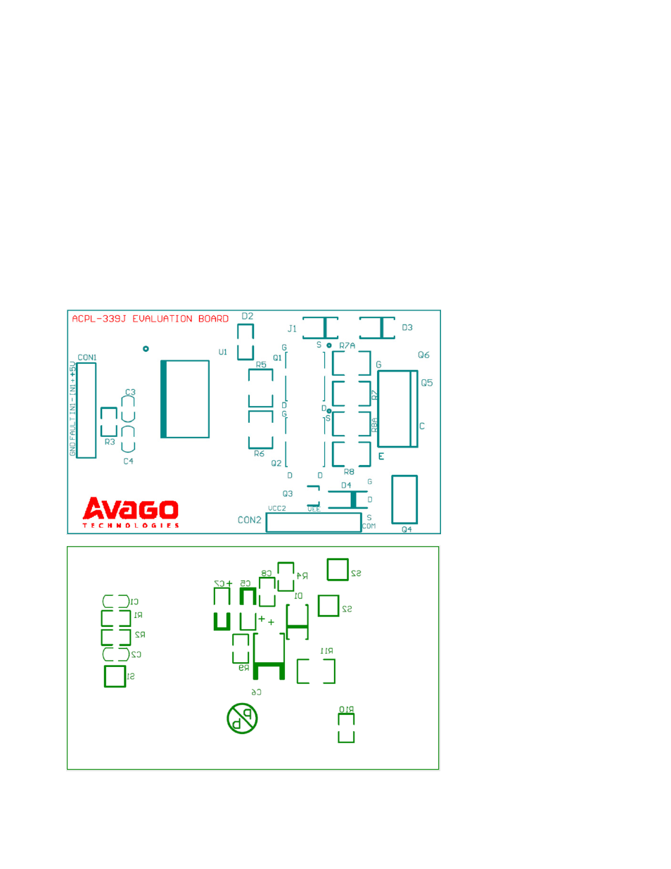
Each of the ACPL-339J evaluation boards (see Figure 4) accommodates an ACPL-339J IC. Two boards are needed to drive
top and bottom arms of the Half-bridge Inverter. It allows the designer to easily test the performance of gate driver in
an actual application under real-life operating conditions. Figure 2 shows the typical de-saturation protected gate drive
circuit that is implemented on the evaluation board. Operation of the evaluation board merely requires the inclusion of
a common 5V DC isolated supply on the input side and two isolated DC supplies (range from 21.6 V ~ 30 V): one for top
arm and one for the bottom arm across V
cc2
and V
ee
. The V
cc2
voltage will then be fixed at +15 V by a Zener diode at D1,
while the balance of the supplied voltage (21.6 V ~ 30 V minus 15 V) will be built across the 1 k
Ω resistor (R11) to set the
negative V
ee
voltage, all with reference to V
e
at each arm.
Note:
As can be seen on the board, the isolation circuitry (at the far left) is easily contained within a small area while maintaining adequate spacing for
good voltage isolation and easy assembly.
Figure 4. Top and Bottom Views of ACPL-339J Evaluation Board
