Schematics, Figure 2. schematics of acpl-339j evaluation board – Avago Technologies ACPL-339J-000E User Manual
Page 2
2
Figure 1. Simple Simulation Test Setup of Evaluation Board
Schematics
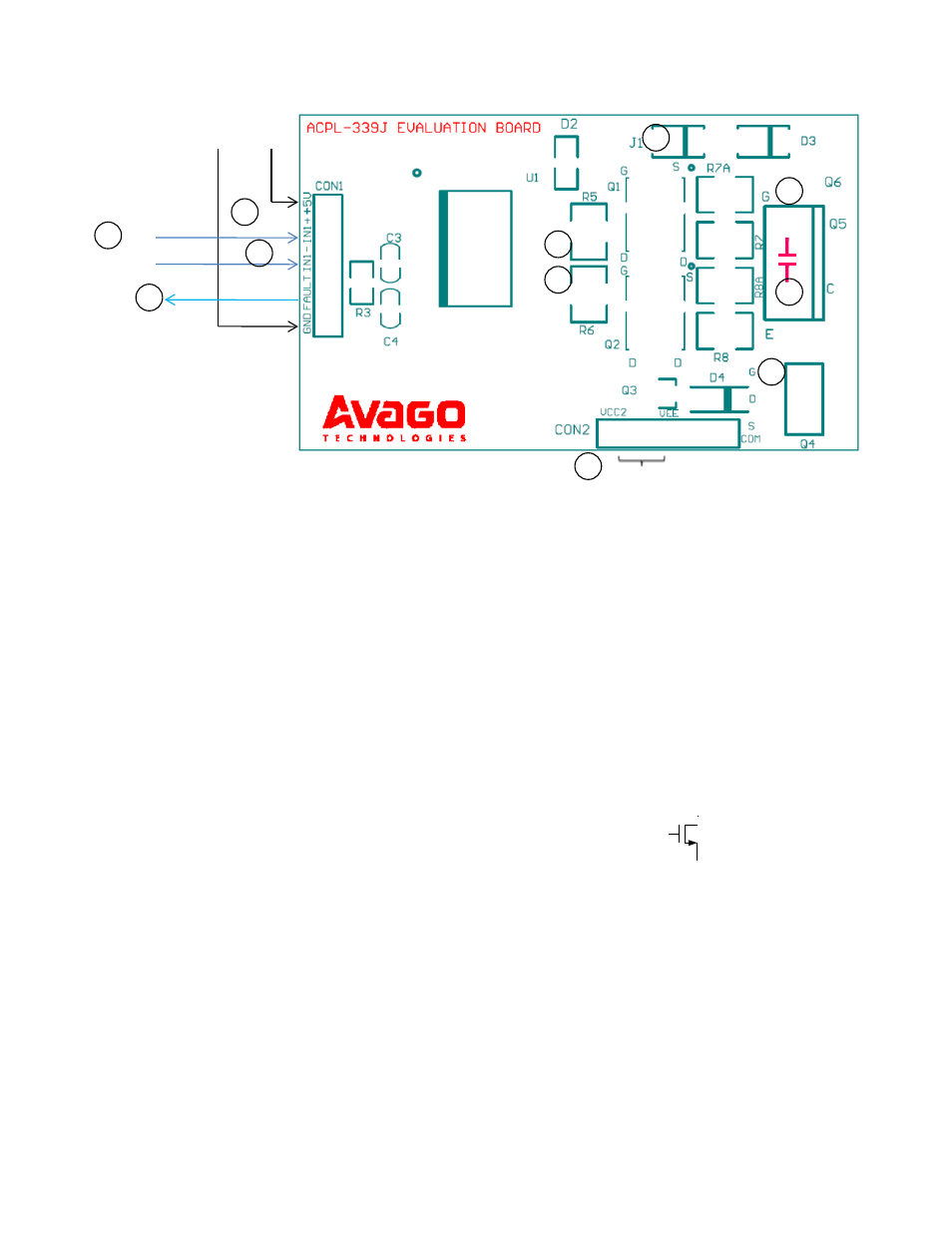
Figure 2 shows the schematics of the Evaluation Board.
2
IN1+
IN1–
Signal Input
4
1
10 nF
21.6 V ~ 30 V
3
5a
5b
5c
5d
5e
5f
5g
DC Supply 2
DC
Su
pp
ly
1
GND
+5V
Figure 2. Schematics of ACPL-339J Evaluation Board
Si2318
1k (½W)
470
R9
R11
Q3
R10
330
ACPL-339J
CATHODE
ANODE
V
GND1
CATHODE
NC
V
CC2
V
GMOS
DESAT
V
OUTP
V
EE
V
OUTN
V
LED
V
CC1
V
E
FAULT
V
GND1
1
2
3
4
5
6
7
8
16
15
14
13
12
11
10
9
Vcc2
+
+
+
Vcc1
GND
IN1+
FAULT
Vcc1
+5V
GND
270
270
10k
1n
330n
220p
G
E
C
Si7465DP
Si7848BDP
15V
100
100p
IGBT (or
Power Mosfet)
(TO-220 & TO-247)
BYM26E
BZG03C15TR3
1µ
Tant
20V
1µ Tant
20V
10µ
Tant
35V
10R (½W)
15 (½W)
15 (½W)
R1
R2
R3
R5
R6
R7//R7a
R8 //R8a
R4
C2
C3
C4
C5
C7
C6
C8
CON1
VE
CON2
C1 220p
IC1
D1
D3
Q1
Q2
NM
J1
Caution: Please
remove S2
jumpers if
IGBT/Power
Mosfet is
connected to
Q5 (or Q6)
VCC2
VEE
VE
VEE
10R (½W)
10R (½W)
10R (½W)
21.6V~30V
VE
VEE
DFLS220L
D2
NM
G
E
C
IN1-
S1
S2
Q5
Q6
- MGA-725M4 (4 pages)
- MGA-71543 (4 pages)
- MGA-71543 (3 pages)
- MGA-82563 (6 pages)
- 3ware SAS 9750-8i (48 pages)
- 3ware 9690SA-8I (Channel) (138 pages)
- 3ware 9690SA-8I (Channel) (380 pages)
- 3ware SAS 9750-8i (29 pages)
- 3ware 9550SXU-8LP (Channel) (149 pages)
- 3ware 9550SXU-8LP (Channel) (40 pages)
- 3ware 9650SE-8LPML (Channel) (45 pages)
- 3ware 9690SA-8I (Channel) (361 pages)
- 3ware 9690SA-8I (Channel) (27 pages)
- 6160 SAS Switch (2 pages)
- MegaRAID SAS 9361-8i (13 pages)
- MegaRAID SAS 9266-8i (12 pages)
- MegaRAID SAS 9380-8e (43 pages)
- Cache Protection for RAID Controller Cards (139 pages)
- Cache Protection for RAID Controller Cards (13 pages)
- MegaRAID SAS 9271-8iCC (13 pages)
- MegaRAID SAS 9285-8ecv (92 pages)
- MegaRAID SAS 9266-8i (20 pages)
- MegaRAID SAS 9271-8iCC (26 pages)
- MegaRAID SafeStore Software (502 pages)
- MegaRAID SAS 9285-8ecv (80 pages)
- MegaRAID SAS 0260CV-4i (64 pages)
- MegaRAID SAS 0260CV-4i (49 pages)
- MegaRAID SAS 9271-8i (8 pages)
- MegaRAID SAS 0260CV-4i (72 pages)
- MegaRAID SAS 9361-8i (7 pages)
- MegaRAID SAS 9341-8i (8 pages)
- MegaRAID SAS 9380-4i4e (7 pages)
- MegaRAID SAS 9380-8e (7 pages)
- MegaRAID SAS 9240-8i (4 pages)
- MegaRAID SAS 0260CV-4i (28 pages)
- MegaRAID SAS 9260-16i (12 pages)
- MegaRAID SAS 9280-24i4e (14 pages)
- MegaRAID SAS 9280-24i4e (16 pages)
- MegaRAID SAS 9260-8i (4 pages)
- MegaRAID SafeStore Software (8 pages)
- MegaRAID SAS 9280-8e (22 pages)
- MegaRAID SAS 9261-8i (4 pages)
- MegaRAID SAS 9285-8e (12 pages)
- MegaRAID SAS 9280-16i4e (12 pages)
- MegaRAID SAS 9280-4i4e (4 pages)