Yaskawa VS606 V74X V7 to V1000 User Manual
Page 25
PL.V1000-4X.01 Transition Guide 6/22/10
Page 25 of 32
Yaskawa America, Inc.
Product Transition Guide
PL. V1000-4X.01 Rev: 6/22/10
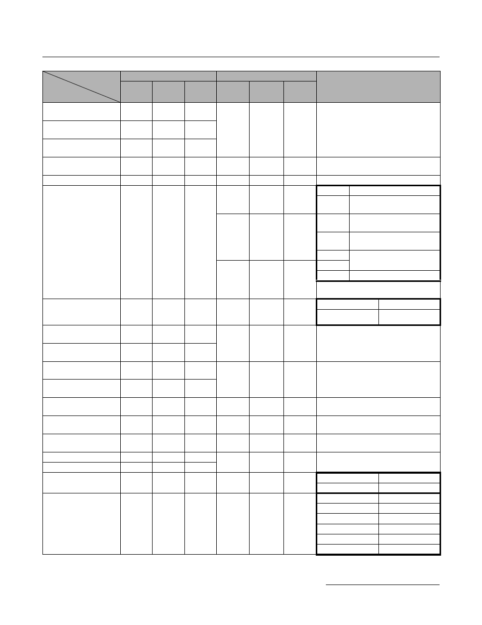
Upper voltage limit for
energy saving at 60Hz
n159
120%
-
-
-
No setting available.
Upper voltage limit for
energy saving at 6Hz
n160
16%
Power detection hold
during voltage tuning
n161
10%
Power detection filter
time constant
n162
5
(20 ms)
b8-05
20 ms
PID output gain
n163
1.0
b5-10
1.0
PID feedback value
selection
n164
0
H3-09
2
V74X
V1000-4X
n164 0
Term. A2:
H3-09 0, H3-10 B
H3-10
0
n164 1
Term. A2:
H3-09 2, H3-10 B
n164 2
Term. A2:
H3-09 3, H3-10 B
n164 3
– (no operator poti)
H6-01
0
n164 4
n164 5
H6-01 = 1
When terminal A2 is used always check
the position of DIP switch S1
Braking resistor over
heat protection
(ERF type)
n165
0
L8-01
0
n165 0
L8-01 0
n165 1
L8-01 1
Input open phase
detection level
n166
0%
L8-05
o2-09
dep.
The input phase loss detection level and
time can not be set in V1000-4X. The
phase loss detection can be enabled/
disabled by setting L8-05.
Input open phase
detection time
n167
0.0 sec
Output open phase
detection level
n168
0%
L8-07
o2-09
dep.
The output phase loss detection level and
time can not be set in V1000-4X. The
phase loss detection can be enabled/
disabled by setting L8-07.
Output open phase
detection time
n169
0.0 sec
Memobus Enter
command selection
n170
0
-
-
V1000-4X accepts Enter commands at
any time.
Frequency reference bias
upper limit (up/down2)
n171
0.0%
d4-08
0.0%
Frequency reference bias
lower limit (up/down2)
n172
0.0%
d4-09
0.0%
DC braking P-gain
n173
83
–
–
–
No need to set up in V1000-4X
DC braking integral time
n174
25
Low speed carrier
frequency reduction
n175
0
L8-38
0
n175 0
L8-38 0
n175 1
L8-38 1
COPY function selection
n176
rdy
o3-01
0
n176 rdy
–
n176 rEd
o3-01 1
n176 CPy
o3-01 2
n176 vFy
o3-01 3
n176 vA
–
n176 Sno
–
Drive
Parameter
Function
V74X
V1000-4X
Note
Param.
No.
Initial
Value
Set
Value
Param.
No.
Initial
Value
Set
Value