Functional description, Input receiver, Fpga delay section – Grass Valley 8916 User Manual
Page 22

16
8916 Instruction Manual
8916 AES/EBU Auto-Tracking Delay DA
Functional Description
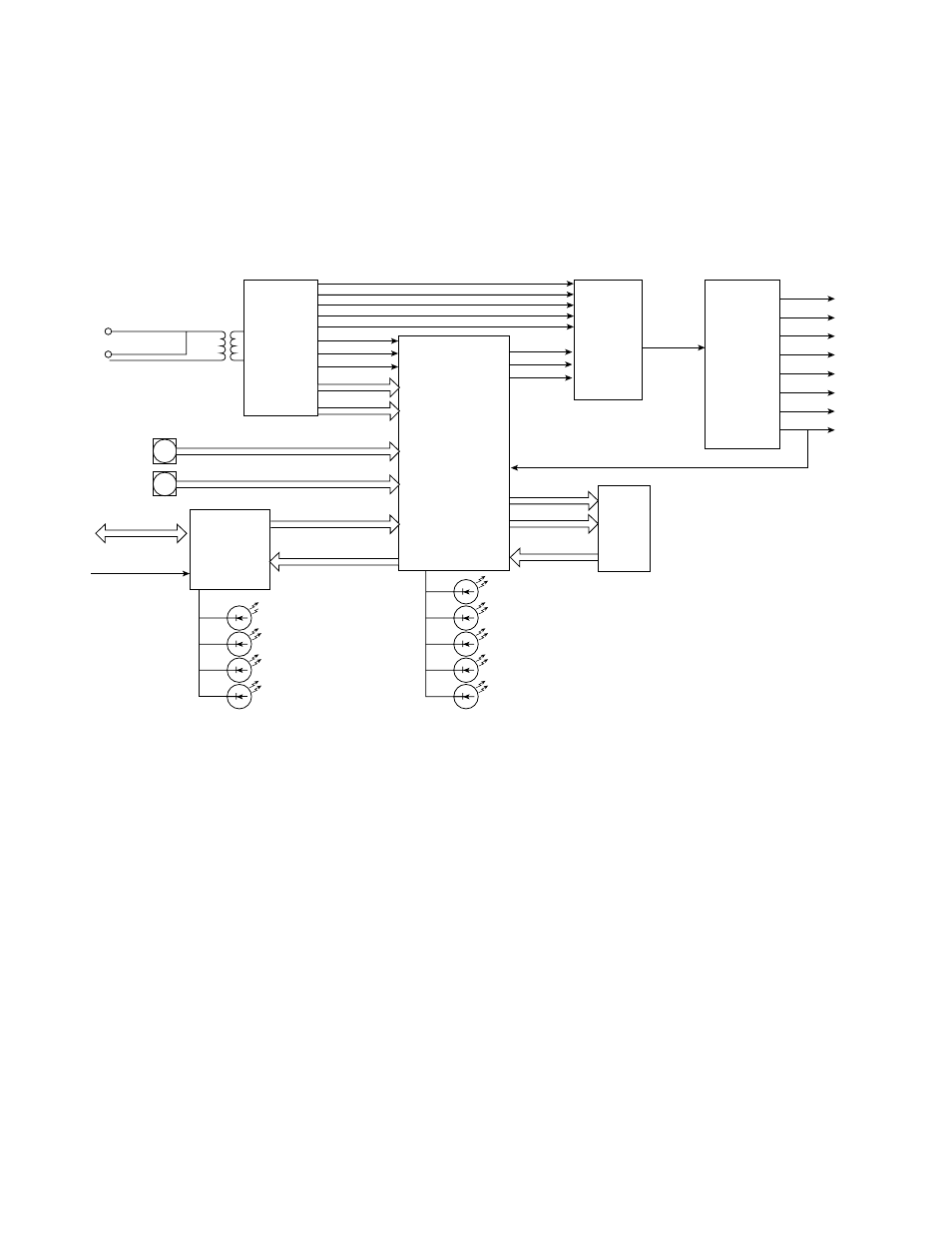
Refer to the block diagram in
while reading the following func-
tional description.
Figure 10. 8916 Block Diagram
Input Receiver
AES/EBU audio data is fed into the 8916 through an isolation transformer
where it is received by the receiver chip. The receiver recovers the clock and
synchronization signals, and demultiplexes the audio and digital data.
FPGA Delay Section
The delay section receives the 12.29 MHz clock, synchronization informa-
tion, frequency information, and error status information. It also receives
the switch position settings that determine the fixed length of delay.
Loop-through
Delay Control I/F
To Host
Fine
Coarse
Delay Select Switches
RS 232
AES/EBU Input
RX+
RX–
Serial Data
SCK
F Sync
Error
Freq.
Serial Data
SCK
Parallel Data
Parallel Data
FIFO
Control
CBL
V
U
C
MCK
F Sync
AES/EBU
Serial
Data
Outputs
32 kHz
44.1 kHz
48 kHz
Tracking
Remote Override
Power
Comm
Fault
Conf
Receiver/
De-MUX
Field
Programmable
Gate Array
(FPGA)
Controller
Line
Drivers
MUX
