Block diagram, Architecture description – Sundance SMT361Q User Manual
Page 7
Version 1.0.2
Page 7 of 24
SMT361Q User Manual
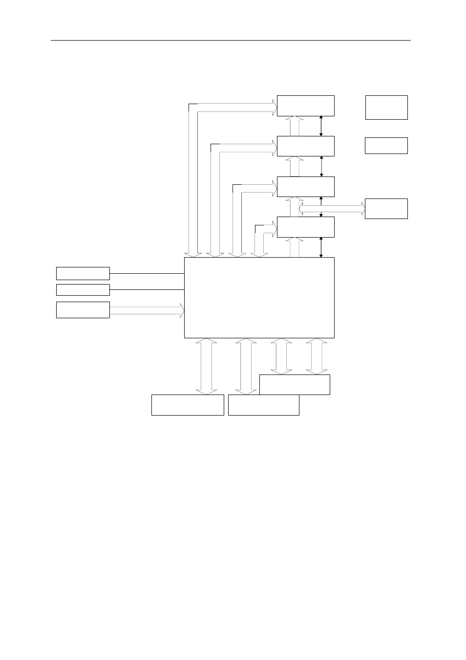
Block Diagram
120 I/O Pins; 16-bit Data
2x
C
o
mm-Port
s
24 I/O p
ins
Ti
m
e
r &
Co
n
tr
o
l
2
x
C
o
m
m
-P
or
ts
24 I
/O
p
ins
Gl
o
b
a
l Bus
74 I
/O
p
ins
FPGA
(XC2V2000)
Virtex-II, FF896
618 I/O Pins
1.5V
'C64xx
DSP
JTAG Header
J1 Top Primary TIM
Connector
Comm-Port 0 & 3
J3 Global Expansion
Connector
J2 Bottom Primary TIM
Connector
Comm-Port 1 & 4
4 LEDs &
4 I/O pins
Flash (CE1)
Oscillators
voltage
convertors
1.5V & 1.2V
Sundance High-
Speed Bus
60-way x2
'C64xx
DSP
'C64xx
DSP
'C64xx
DSP
HPI
HPI
HPI
HPI
Serial port
16
b
it
EMI
F
A
E
MI
F
A
EM
IFA
E
MI
F
A
32
b
it
32
b
it
32
b
it
32
b
it
EMIFB
EMIFB
EMIFB
A
B
C
D
Architecture Description
The SMT361Q TIM consists of a Texas Instruments TMS320C6416 running at
600MHz.
A Field Programmable Gate Array (FPGA) is used to manage Global bus accesses
and implement four ComPorts and two Sundance High Speed Busses. This is a
Xilinx Virtex-II device.
- SMT107 (16 pages)
- SMT6035 v.2.2 (39 pages)
- SMT6012 v.4.6 (22 pages)
- FC100 (12 pages)
- FC108 v.1.1 (10 pages)
- SMT6065 v.4.0 (45 pages)
- FFT v.2.1 (19 pages)
- SMT111 (18 pages)
- SMT118LT (10 pages)
- SMT118 (20 pages)
- SMT123-SHB (13 pages)
- SMT128 (15 pages)
- SMT145 (18 pages)
- SMT148 (35 pages)
- SMT130 v.1.0 (46 pages)
- SMT148FX (48 pages)
- SMT310Q (55 pages)
- PARS (70 pages)
- SMT166-FMC (52 pages)
- SMT166 (44 pages)
- SMT300Q v.1.6 (61 pages)
- SMT310 v.1.6 (50 pages)
- SMT317 (24 pages)
- SMT326v2 (24 pages)
- SMT338 (19 pages)
- SMT349 (32 pages)
- SMT339 v.1.3 (27 pages)
- SMT338-VP (22 pages)
- SMT358 (25 pages)
- SMT351T (37 pages)
- SMT351 (25 pages)
- SMT350 (45 pages)
- SMT362 (30 pages)
- SMT365G (23 pages)
- SMT364 (37 pages)
- SMT373 (15 pages)
- SMT368 (24 pages)
- SMT370v3 (46 pages)
- SMT377 (22 pages)
- SMT381 2007 (31 pages)
- SMT381-VP (81 pages)
- SMT387 (42 pages)
- SMT391 (18 pages)
- SMT384 (47 pages)
- SMT390-VP (55 pages)