Connector pinouts, Fpga prog pin control (jp1), Fpga jtag (jp2) – Sundance SMT361Q User Manual
Page 19: Ttl (jp3)
Version 1.0.2
Page 19 of 24
SMT361Q User Manual
Connector Pinouts
FPGA PROG Pin Control (JP1)
The FPGA PROG pin is used to clear the FPGA configuration.
It is to be used as a safety in case the FPGA has been programmed with a bad
bitstream that corrupts the dsp external bus and prevents which any further
programming. Removing the jumper allows the user to clear the FPGA configuration
and reprogram the FPGA. A jumper must always be fitted for proper operation.
FPGA JTAG (JP2)
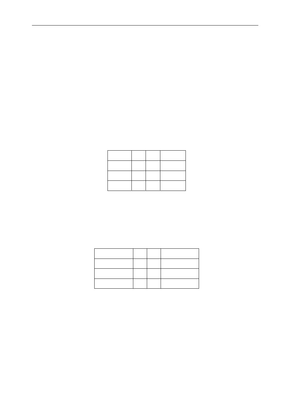
The following shows the pin-outs for JP2 (FPGA) JTAG connector:
Signal Pin
Pin
Signal
V33 1 2 TCK
GND
3
4
TMS
TDO 5 6 TDI
TTL (JP3)
The following shows the pin-outs for JP3 TTL connector:
Signal Pin Pin
Signal
V33 1
2
TTL
DSP_A
TTL DSP_D
3
4
TTL DSP_C
TTL DSP_B
5
6
GND
- SMT107 (16 pages)
- SMT6035 v.2.2 (39 pages)
- SMT6012 v.4.6 (22 pages)
- FC100 (12 pages)
- FC108 v.1.1 (10 pages)
- SMT6065 v.4.0 (45 pages)
- FFT v.2.1 (19 pages)
- SMT111 (18 pages)
- SMT118LT (10 pages)
- SMT118 (20 pages)
- SMT123-SHB (13 pages)
- SMT128 (15 pages)
- SMT145 (18 pages)
- SMT148 (35 pages)
- SMT130 v.1.0 (46 pages)
- SMT148FX (48 pages)
- SMT310Q (55 pages)
- PARS (70 pages)
- SMT166-FMC (52 pages)
- SMT166 (44 pages)
- SMT300Q v.1.6 (61 pages)
- SMT310 v.1.6 (50 pages)
- SMT317 (24 pages)
- SMT326v2 (24 pages)
- SMT338 (19 pages)
- SMT349 (32 pages)
- SMT339 v.1.3 (27 pages)
- SMT338-VP (22 pages)
- SMT358 (25 pages)
- SMT351T (37 pages)
- SMT351 (25 pages)
- SMT350 (45 pages)
- SMT362 (30 pages)
- SMT365G (23 pages)
- SMT364 (37 pages)
- SMT373 (15 pages)
- SMT368 (24 pages)
- SMT370v3 (46 pages)
- SMT377 (22 pages)
- SMT381 2007 (31 pages)
- SMT381-VP (81 pages)
- SMT387 (42 pages)
- SMT391 (18 pages)
- SMT384 (47 pages)
- SMT390-VP (55 pages)