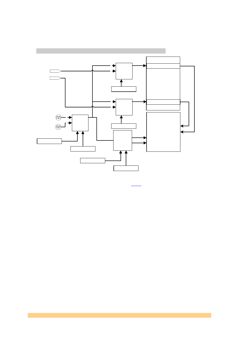
2 description of the clock tree controls, Figure 5: clock tree controls, Fpga – Sundance SMT791 User Manual
Page 14

the firmware structure to allow the modifications or the replacement of blocks
without having features intertwined and requiring a re-design everytime a feature
needs to be altered.
4.4.2 Description of the Clock Tree Controls
AT84AD001B
S
1
S
2
D
C
ENB
Multiplexer
CLKSRCMUXRST
clksrc_pins_sel
0
S
1
S
2
D
C
ENB
Multiplexer
S
1
S
2
D
C
ENB
Multiplexer
0
0
1
1
adcI_pins_clksrc
adcQ_pins_clksrc
Channel I clk
Channel Q clk
CLKSYNTH
VCO
1
External Clock Channel I
External Clock Channel Q
Clk Div 8
div8_pins_reset
div8_pins_nEn
FPGA
nEn
Rst
Rst
En
Rst
En
En
Rst
Figure 5: Clock tree controls
The main clock source of the module is a
600MHz to 1000MHz voltage
controlled oscillator. The frequency range of the VCO is adjustable with a National
PLL. The output of the VCO + PLL combination is passed through a Maxim high
frequency comparator with an LVPECL output to form the main system clock.
In addition to this clock there is a clock synthesizer on the module that can
generate a 50 to 950 MHz clock. This clock is ideal for testing purposes as it spans a
wider frequency range, but it is less clean than the VCO+PLL combination.
Alternatively the user can provide the module with an external LVPECL clock, one
input for each channel.
The FPGA controls the LVPECL multiplexers which route the final clock to the ADC
(clock synthesizer, PLL+VCO, or external). A copy of this clock is fed to each channel
of the ADC.
A copy of the internal clock selected is divided by 8 (so if the PLL is selected to be
the internal clock and set up at 1000 MHz, then the copy gives a 125MHz LVPECL
clock) and fed into the FPGA. (In the current firmware implementation this copy of
the clock is not used by the firmware design. The two clocks originating from the
ADC are used by the design).
Note that the external clock for a channel does not follow the same path as the
internal clocks.
User Manual SMT791
Page 14 of 14
Last Edited: 12/10/2010 09:52:00
