3 digital data stream description – Sundance SMT791 User Manual
Page 12

4.3 Digital Data Stream Description
The data-path for both channels on the mezzanine and in the FPGA is identical. The
ADC is driven by a clock either generated on the mezzanine (one clock for both
channels) or provided by the user through MMBX connectors (one clock for each
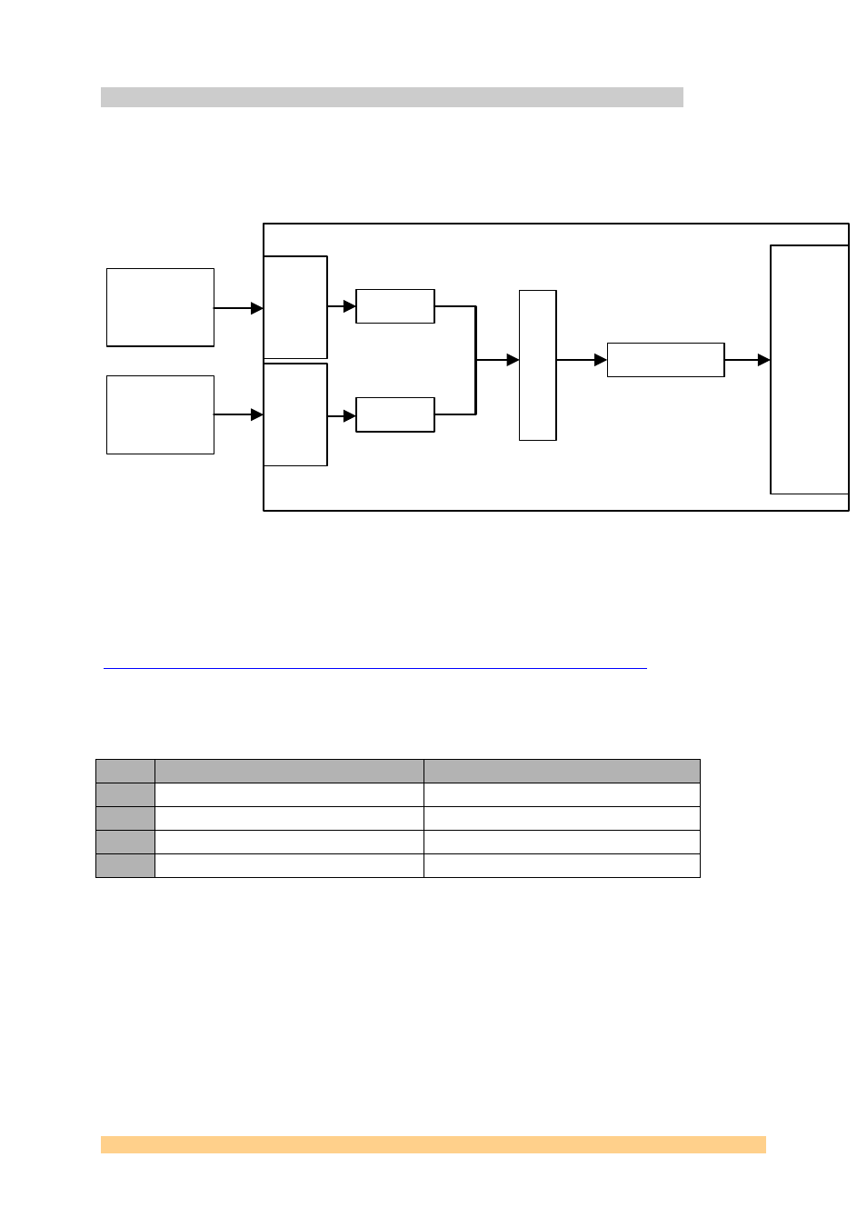
channel). The following figure is a diagrammatic representation of the data-path
inside the FPGA.
ADC
Channel Data A
XLINK for Channel
Fifo
Input
delay
calibration
unit
DDR Data
Recapture
DDR Data
Recapture
ADC
Channel Data B
Input
delay
calibration
unit
PCIe
Interface
Figure 3: FPGA Data path for one Channel, Channel I or Channel Q.
The ADC sends an image of the sampling clock (Fs/4) with the data in DDR mode,
on both I and Q channels. The data timing versus the clock is detailed in figure 4.2
p.12 of the ADC User Guide:
The following table shows how the output data of the ADC is encoded:
Description
Binary Value (8 Bits)
1
Positive full scale is 255
"11111111"
2
Bipolar zero +1/2 LSB is 128
"10000000"
3
Bipolar zero -1/2 LSB is
"01111111"
4
Negative full scale is 0
"00000000"
Figure 4: ADC Data Output.
User Manual SMT791
Page 12 of 12
Last Edited: 12/10/2010 09:52:00
