Jtag cabling, Table 19 : buffered comport connector pin out – Sundance SMT410 v.1.0 User Manual
Page 47
Page 47 of 49
SMT410 User Manual V1.0
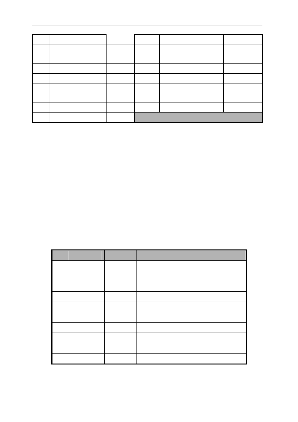
6 3 GND
GND 20 10
D7
D7
7 4 /CRDY
/CRDY
21 11 VCC
VCC
8 4 GND
GND 22 11 GND
GND
9 5 /CREQ
/CREQ
23 12
/RST_OUT
/RST_IN
10 5 GND GND 24 12 GND
GND
11 6 /CACK
/CACK
25 13 /RST_IN
/RST_OUT
12 6 GND GND 26 13 GND
GND
13 7
D0 D0
SHELL - SHIELD SHIELD
14 7
D1 D1
Table 19 : Buffered ComPort connector pin out
The overall shield is attached to the body of the metal plug shell.
The signal VCC is fused on the board at 1 amp; it automatically resets when the load
is removed.
When the buffered ComPort is reset to input, pins 1 and 23 are always driven and
pins 3 and 25 are always receivers. When the buffered ComPort is reset to output,
pins 3 and 25 are always driven and pins 1 and 23 are always receivers.
17.3 JTAG cabling
Internal JTAG (XDS-510 compatible) pin header pin information:
J31
Pin
Signal
Direction
Description
1
TMS
Out
JTAG Test mode select
2 /TRST Out
JTAG Reset
3 TDI
Out
JTAG data out
4 GND
5 PD
(+5)
XDS_OUT detect
6 Key
5v
Power
7 TDO
In
JTAG data in
8 GND
9 TCK_RET
In
JTAG clock return
10 GND