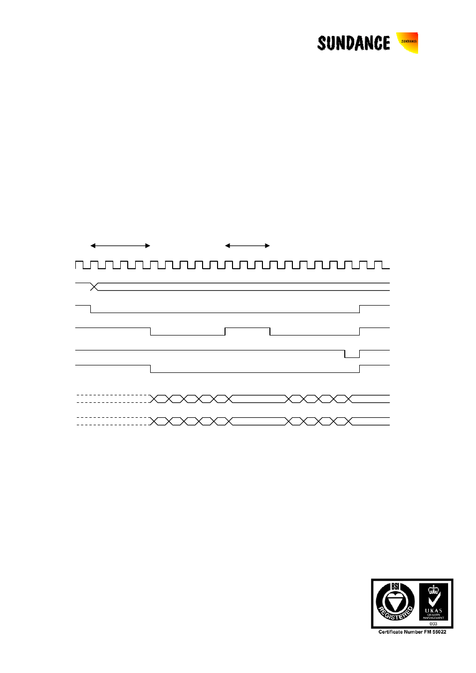
Figure 6 : timing diagram for dsp local bus access, Dsp’s global bus address lines, Dsp’s global bus data lines – Sundance SMT410 v.1.0 User Manual
Page 32
User Manual (QCF42); Version 3.0, 8/11/00; © Sundance Multiprocessor Technology Ltd. 1999
LCLK
STRB1
RDY1
STAT0
AE/DE
A[30..0]
D[31..0]
A0..A30
DSP’s global Bus address lines
D0..D31
DSP’s global Bus data lines
IIOF0, IIOF1 & IIOF2
DSP’s Interrupt signals. These are open collector signals on the SMT410. They can
be driven by the DSP to generate an interrupt to the host, or they can be driven by
the host to interrupt the DSP.
In the timing diagram below all signals change relative to the rising LCLK signal. This
signal is the H1 clock signal of the DSP when using the DSP global bus in
synchronous mode (see SMT335 User Guide).
Figure 6 : Timing diagram for DSP local bus access
* LCLK Period =30nS, frequency is 33MHz.
The DSP initiates a global bus R/W by asserting the STRB1 low and STAT[1:3}
change (see TIM Spec for details of STAT[1..3] details). Once the arbitration unit
detects this, it waits for the last cycle of the Local bus to be completed by the PCI
Bridge, before allowing the DSP to become Bus Master. Once the DSP is Master the
arbitration unit drives AE and DE low to enable the DSP’s address and data lines.
RDY1 is driven low by the arbitor to indicate to the DSP, on the next rising LCLK, that
the data packet has been transferred. If the input FIFO (256 Words Deep) becomes
STAT[1.3]
TIMReq FIFO
Full