System ace sc – Sundance SMT498 User Manual
Page 33
System ACE SC
To configure the FPGA from the Flash on power up, install the jumper pin near the
PROM chip. Turn the switch 1 of S2 to ‘ON’ position and switch 2 of S2 to ‘OFF’
position. Switch 4 of S3 should be in ‘OFF’ position for the JTAG to work and
switches 1, 2, and 3 should be in the ‘ON’ position.
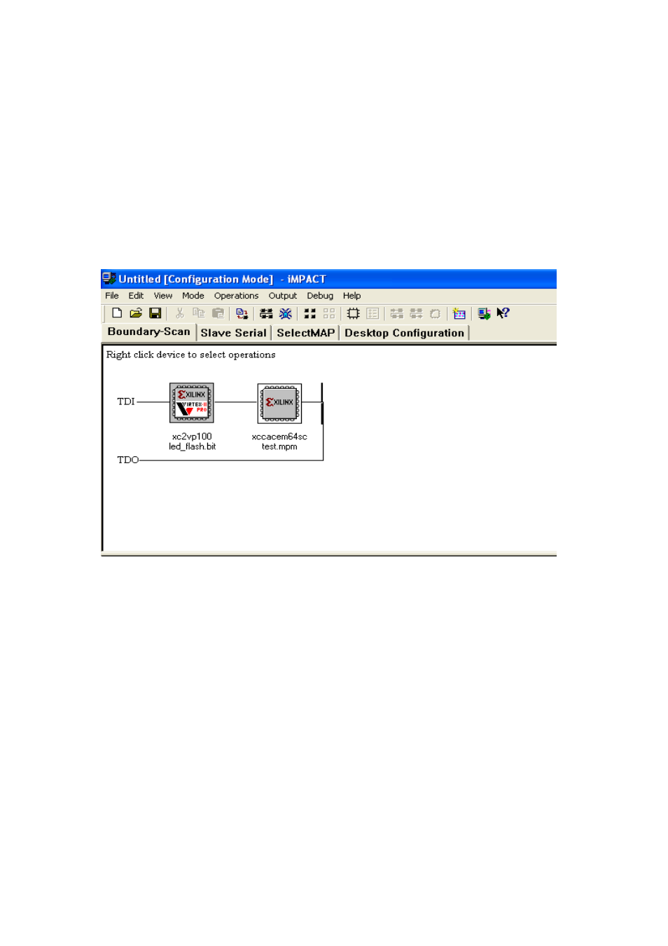
To initialize the JTAG chain, connect the Xilinx Parallel cable to JTAG IN connector
JA2. Using the Xilinx impact software initialize the JTAG chain, this will show two
devices as shown in the figure below
The first device will be the XC2VP100 and the second device will be XCCACEM64
SC (this is the System ACE chip that allows the bitstream to be loaded into the flash
via JTAG). Assign the .MPM file (Generation of the .MPM file is given at the end) to
the System ACE chip and program it. To check the configuration of the VP100 via
the Flash, toggle the switch 4 of S3 this will reset the system ACE and configure the
FPGA from the Flash. You will see the done pin (LED D5, which is not populated on
the prototype) of the Target FPGA go low. This confirms the FPGA is configured and
you will see the status LED’s D12, D13 lit. From now onwards as soon as the board
is powered up the VP100 will be configured from Flash.
Note: In this mode the VP100 cannot be configured directly via the JTAG.
Page 33