Virtex ii fpga, Fpga block diagram, Configuration – Sundance SMT498 User Manual
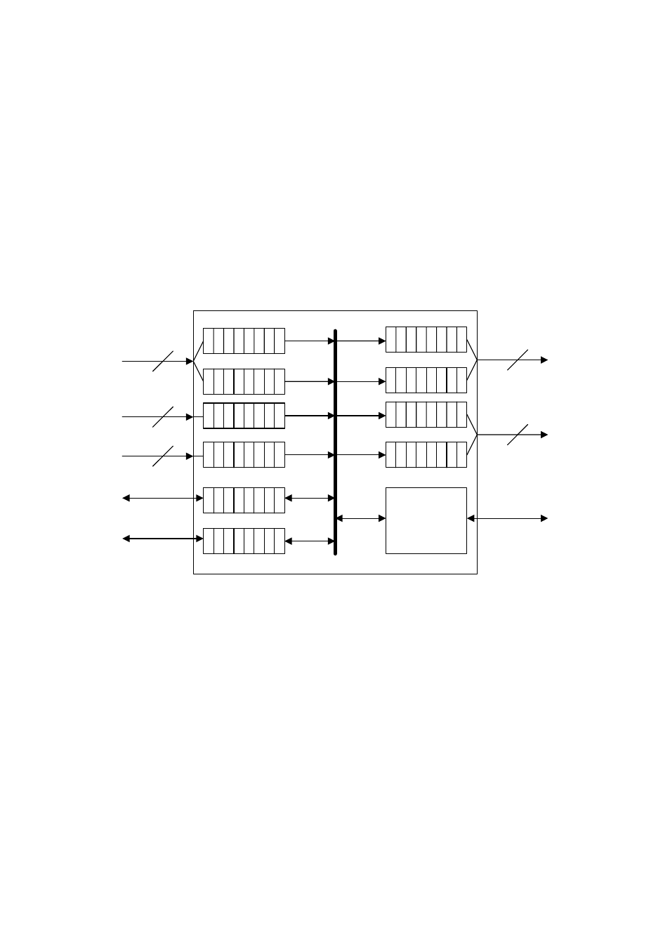
Page 12: Memory, Figure 4 - default fpga configuration

Virtex II FPGA
The module can be fitted with an XC2VP70 or XC2VP100 FPGA. Only flip-chip
FF1152 package will fit on this board. The choice of FPGA will be price/performance
driven.
This Xilinx Virtex II Pro, is responsible for the provision of 5 SHBs, 2 Comports via
the SHB user IO pins, a PCI Local bus interface, and 14 RSLs (see Ordering
Information).
FPGA Block Diagram
SHBA
60
16-bit SDB
16-bit SDB
SHBB
60
32-bit SDB
SHBC
60
16-bit SDB
16-bit SDB
SHBD
60
16-bit SDB
16-bit SDB
Local Bus
Interface
Comport
Comport
Comport A
Comport B
QuickLogic
SHBE
60
32-bit SDB
Figure 4 - Default FPGA Configuration
Configuration
The FPGA can be configured in three different ways:
•Loading the FPGA on power up from flash on the board using System ACE SC.
•Using the SMT6041-498 utility to load the FPGA over the PCI bus.
•Using the on-board JTAG header and Xilinx JTAG programming tools.
(See the Appendix for full details)
Memory
Two banks of DDR SDRAM are attached directly to the FPGA for storage of
incoming data. Each bank consists of two 133 MHz DDR SDRAM components
(Micron MT46V32M16FN or equivalent) providing a total of 128 MB of storage
capacity on the module.
Page 12
