Clocks, Clocks pci, Figure 7: fpga pci command sequences – Sundance SMT387 User Manual
Page 23: Table 4: fpga pci register offsets

Version 1.0.3
Page 23 of 42
SMT387 User Manual
Clocks
The FPGA clock is provided by the EMIFA of the DSP. This can be configured as ¼
or 1/6 of the DSP core speed (e.g. if the DSP core speed is 600MHz, the FPGA is
running at 100MHz by default).
There is a place to install an oscillator of a different frequency on the PCB, but keep
in mind that this clock will also be used for the SDRAM.
PCI
The FPGA PCI interface is required to perform byte-oriented reads and writes over
the PCI bus.
The following are the offsets of the associated PCI registers:
Address PCI
Function
0xB0060000 FPGA_PCI_CMD
0xB0068000 FPGA_PCI_ADDR
0xB0070000 FPGA_PCI_DOUT
0xB0078000 FPGA_PCI_DIN
Table 4: FPGA PCI Register Offsets
Set
FPGA_PCI_CMD
Reset bit
Wait 1ms
Clear
FPGA_PCI_CMD
Reset bit
Set
FPGA_PCI_CMD
IDSEL
Perform PCI
configuration via
DSP PCI interface
Write
FPGA_PCI_ADDR
Write
FPGA_PCI_DATA
Clear
FPGA_PCI_CMD
IDSEL
Reset
Configuration
I/O Read
Write
FPGA_PCI_ADDR
I/O Write
Set
FPGA_PCI_CMD
= 0x2
Poll for
FPGA_PCI_CMD
Idle
Read from
FPGA_PCI_DATA
Set
FPGA_PCI_CMD
= 0x3
Poll for
FPGA_PCI_CMD
Idle
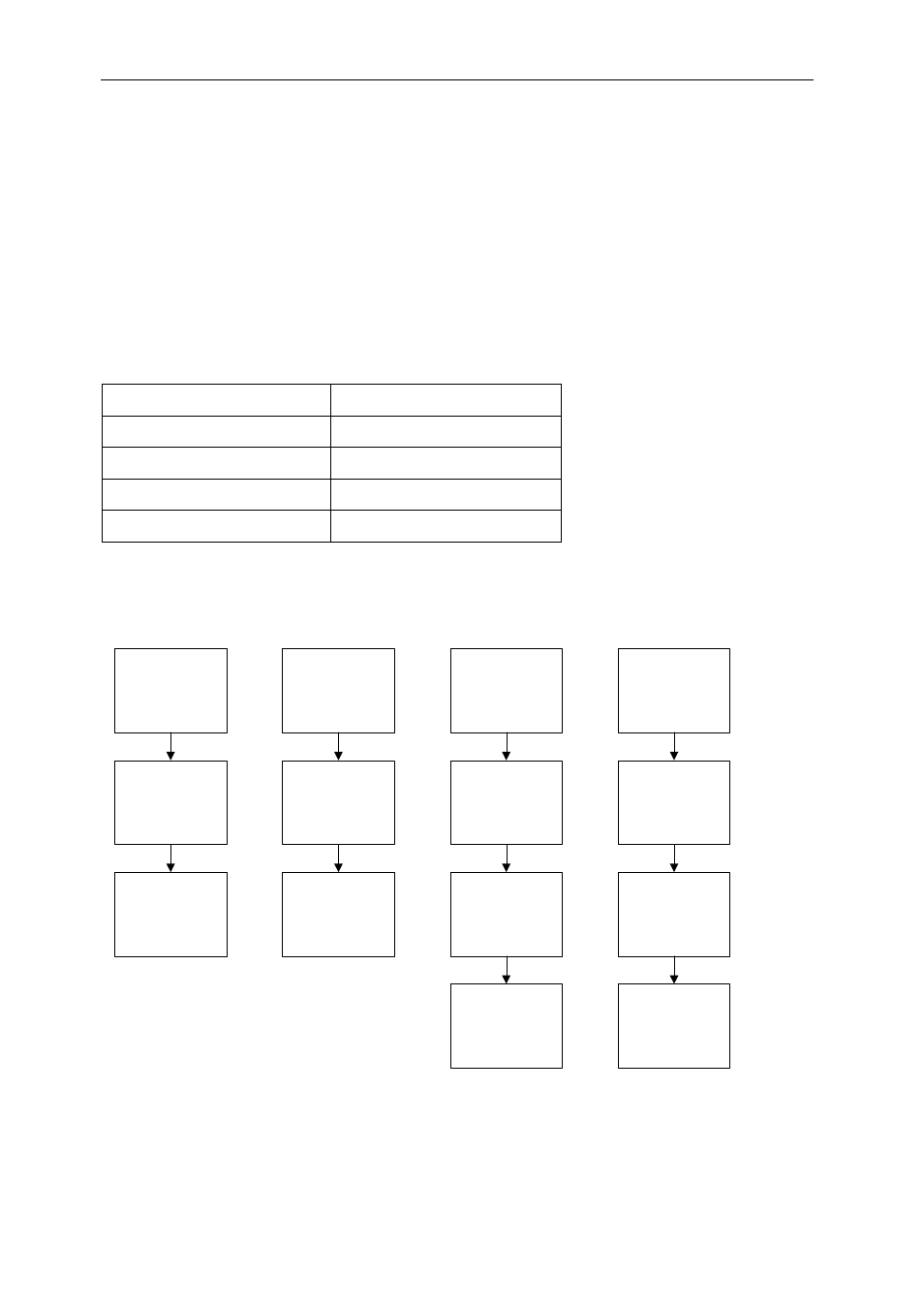
Figure 7: FPGA PCI Command Sequences
