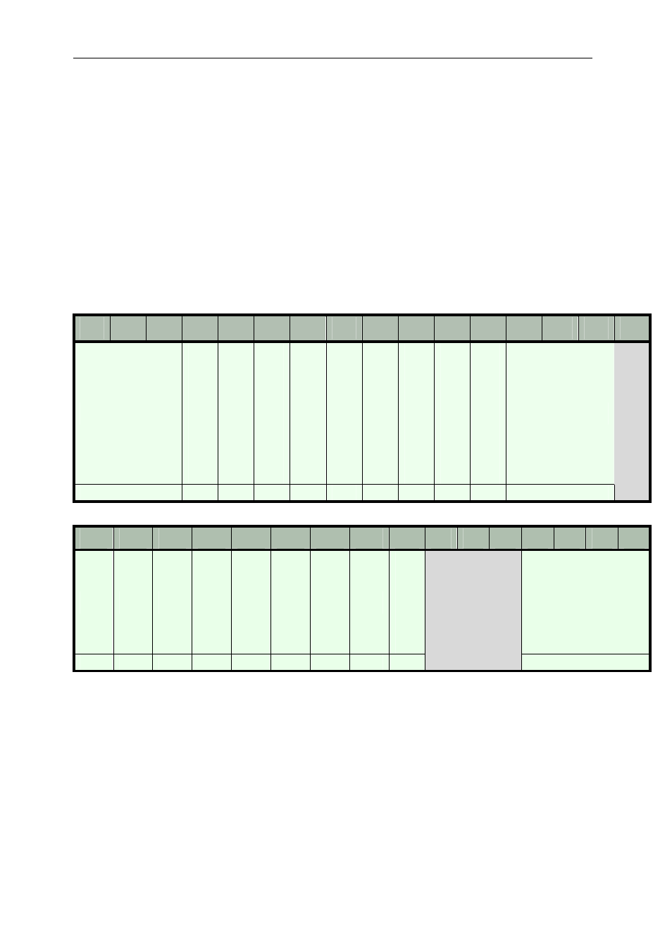
Adc control, Figure 4: adcs control register – Sundance SMT317 User Manual
Page 13

Version 6.1
Page 13 of 24
SMT317 User Manual
The buffered external clock is used directly as the ADCs sample clock.
13.
ADC Control
All of the ADCs are controlled via the comm-port 3. The comm-port 3 must be
selected using the jumper bank
JMP1: Control Comm-port Select.
The ADC control is provided by configuring a single control register. It allows control
for the clock divider, the clock selection, the trigger source, the mode (), the ADC
enable and the state of three LEDs. This register is described here,
31
30
29
28
27
26
25
24
23
22
21
20
19
18
17
16
Count_data_fifo
Trigger_int
Internal trig
ger
Active trigger level
Continuous
mode
Half pwr
Internal Sync
Mode 1
Mode 0
EXT Clock
LED [4:2]
W,000
W,0
W,0
W,0
W,0
W,0
W,0
W,0
W,0
W,0
W,000
Extra Count_data_fifo
bit
15
14
13
12
11
10
9
8
7
6
5
4
3
2
1
0
CH7 CH3 CH6 CH2 CH5 CH1 CH4 CH0
Rst SDB
CLK DIV
W,0
W,0
W,0
W,0
W,0
W,0
W,0
W,0
W,0
Not Used
W,0000
Figure 4: ADCs control register
