Channel switching error – Measurement Computing USB-2416-4AO User Manual
Page 35
USB-2416-4AO User's Guide
Specifications
35
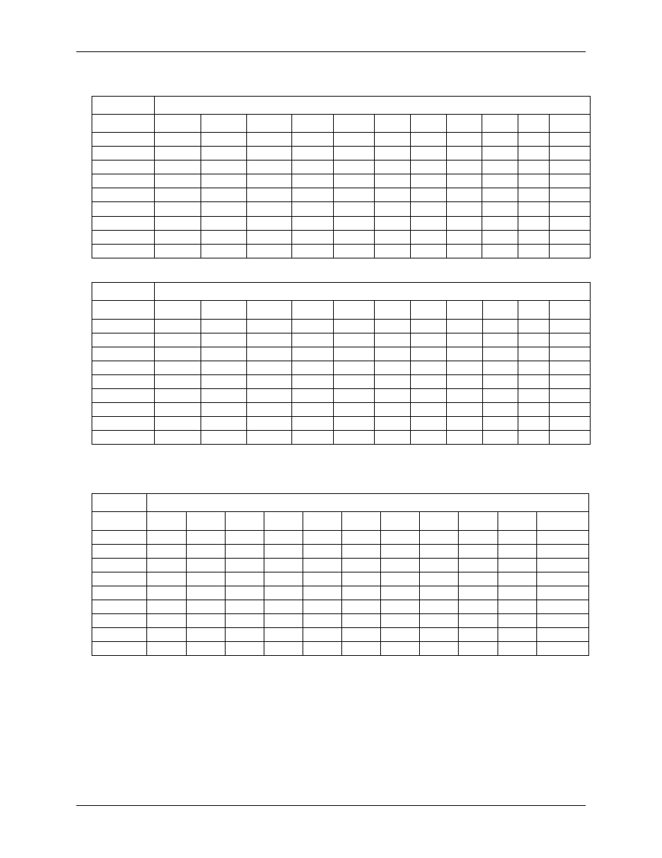
Table 15. RMS noise performance specifications (µVRMS)
A/D data rate
Range
3750 S/s
2000 S/s
1000 S/s
500 S/s
100 S/s
60 S/s
50 S/s
25 S/s
10 S/s
5 S/s
2.5 S/s
±20 V
34.90
28.32
19.22
15.17
8.67
8.67
7.51
7.22
3.61
3.61
2.17
±10 V
19.22
15.17
10.87
6.83
4.62
4.62
4.05
2.89
1.81
1.44
1.44
±5 V
8.60
7.21
5.18
3.92
2.46
2.17
2.17
2.16
0.90
0.72
0.72
±2.5 V
4.99
4.36
2.72
2.15
1.14
1.07
1.07
0.87
0.58
0.43
0.36
±1.25 V
2.81
2.66
2.10
1.41
0.83
0.83
0.76
0.58
0.51
0.51
0.43
±0.625 V
2.86
2.51
1.28
1.12
0.81
0.73
0.66
0.58
0.38
0.40
0.30
±0.3125 V
2.32
2.24
1.24
1.05
0.72
0.71
0.68
0.56
0.51
0.39
0.37
±0.15625 V
2.01
2.55
1.13
1.00
0.86
0.68
0.68
0.64
0.40
0.47
0.35
±0.078125 V
2.04
2.28
1.39
1.04
0.65
0.63
0.60
0.54
0.35
0.32
0.36
Table 16. Noise-free resolution specifications (bits)
A/D data rate
Range
3750 S/s
2000 S/s
1000 S/s
500 S/s
100 S/s
60 S/s
50 S/s
25 S/s
10 S/s
5 S/s
2.5 S/s
±20 V
17.4
17.7
18.2
18.6
19.4
19.4
19.6
19.6
20.6
20.6
21.4
±10 V
17.2
17.6
18.1
18.7
19.3
19.3
19.5
20.0
20.6
21.0
21.0
±5 V
17.4
17.6
18.1
18.5
19.2
19.4
19.4
19.4
20.6
21.0
21.0
±2.5 V
17.2
17.4
18.1
18.4
19.3
19.4
19.4
19.7
20.3
20.7
21.0
±1.25 V
17.0
17.1
17.4
18.0
18.8
18.8
18.9
19.3
19.5
19.5
19.7
±0.625 V
16.0
16.2
17.1
17.3
17.8
18.0
18.1
18.3
18.9
18.8
19.2
±0.3125 V
15.3
15.3
16.2
16.4
17.0
17.0
17.0
17.3
17.5
17.9
17.9
±0.15625 V
14.5
14.1
15.3
15.5
15.7
16.1
16.1
16.1
16.8
16.9
17.1
±0.078125 V
14.5
14.3
15.0
15.4
16.1
16.2
16.2
16.4
17.0
17.1
16.9
Channel switching error
Table 17. Step response accuracy specifications
Accuracy
Range
3750 S/s 2000 S/s 1000 S/s 500 S/s 100 S/s
60 S/s
50 S/s
25 S/s
10 S/s
5 S/s
2.5 S/s
±20 V
0.0011% 0.0006% 0.0004% 0.0003% 0.0002% 0.0002% 0.0002% 0.0002% 0.0001% 0.0001% 0.0001%
±10 V
0.0010% 0.0008% 0.0005% 0.0004% 0.0002% 0.0002% 0.0003% 0.0002% 0.0001% 0.0001% 0.0001%
±5 V
0.0009% 0.0008% 0.0004% 0.0004% 0.0003% 0.0002% 0.0002% 0.0002% 0.0001% 0.0001% 0.0001%
±2.5 V
0.0010% 0.0007% 0.0008% 0.0004% 0.0003% 0.0002% 0.0002% 0.0002% 0.0002% 0.0001% 0.0001%
±1.25 V
0.0013% 0.0009% 0.0008% 0.0007% 0.0004% 0.0004% 0.0003% 0.0003% 0.0003% 0.0003% 0.0003%
±0.625 V
0.0022% 0.0016% 0.0011% 0.0011% 0.0007% 0.0007% 0.0005% 0.0005% 0.0004% 0.0005% 0.0003%
±0.3125 V
0.0031% 0.0031% 0.0020% 0.0017% 0.0015% 0.0012% 0.0010% 0.0010% 0.0012% 0.0009% 0.0009%
±0.15625 V
0.0056% 0.0062% 0.0048% 0.0037% 0.0032% 0.0025% 0.0024% 0.0021% 0.0019% 0.0022% 0.0016%
±0.078125 V
0.0114% 0.0123% 0.0076% 0.0070% 0.0041% 0.0051% 0.0046% 0.0036% 0.0032% 0.0030% 0.0034%
Channel switching error is defined as the accuracy that can be expected after one conversion when switching
from a channel with a DC input at one extreme of full scale to another channel with a DC input at the other
extreme of full scale, expressed in terms of percentage of full scale value.