Using the board test system, The configure menu, The config tab – Altera Arria II GX FPGA User Manual
Page 24: Board information, Using the board test system –4, The configure menu –4 the config tab –4, Board information –4
6–4
Chapter 6: Board Test System
Using the Board Test System
Arria II GX FPGA Development Kit, 6G Edition User Guide
July 2010
Altera Corporation
1
If you power up your board with the USR LOAD switch (SW4.4) in the off position, or
if you load your own design into the FPGA with the Quartus II Programmer, you
receive a message prompting you to configure your board with a valid Board Test
System design. Refer to
for information about configuring
your board.
Using the Board Test System
This section describes each control in the Board Test System application.
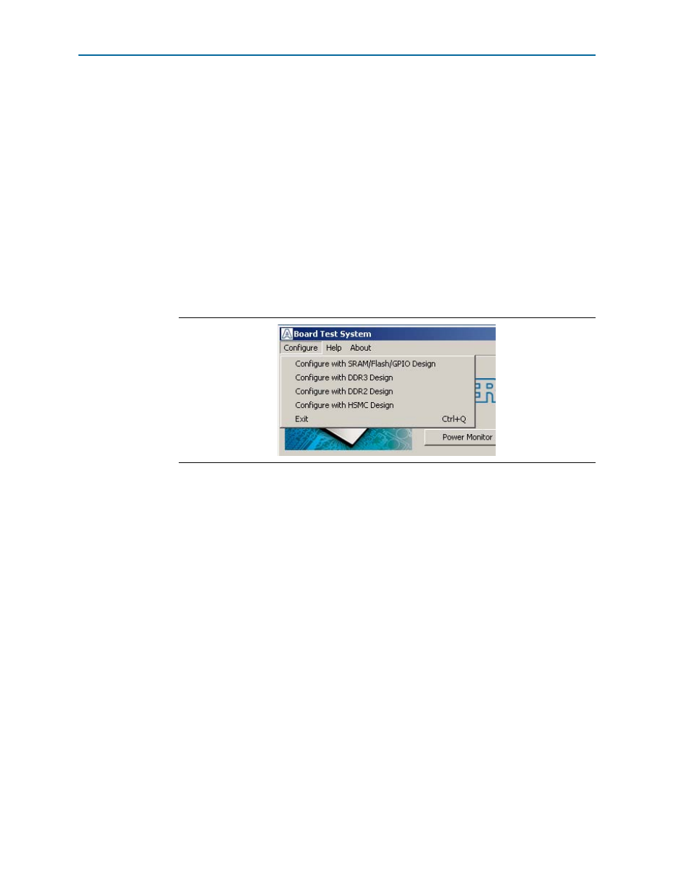
The Configure Menu
Each test design tests different functionality and corresponds to one or more
application tabs. Use the Configure menu to select the design you want to use.
shows the Configure menu.
To configure the FPGA with a test system design, perform the following steps:
1. On the Configure menu, click the configure command that corresponds to the
functionality you wish to test.
2. In the dialog box that appears, click Download Start to download the
corresponding design’s SRAM Object File (.sof) to the FPGA. The download
process usually takes about a minute.
3. When configuration finishes, close the Quartus II Programmer. The design begins
running in the FPGA. The corresponding GUI application tabs that interface with
the design enable.
The Config Tab
The Config tab shows information about the board’s current configuration.
shows the Config tab. The tab displays the contents of the
MAX II registers, the JTAG chain, the board’s MAC address, the flash memory map,
and other details stored on the board.
The following sections describe the controls on the Config tab.
Board Information
The Board information controls display static information about your board.
Figure 6–2. The Configure Menu