3 operations, 1 functional block diagram, 2 analog input channel – ADLINK PXIe-9529 User Manual
Page 23: 1 analog input front-end configuration, Functional block diagram, Analog input channel, Analog input front-end configuration, Figure 3-1, Analog input architecture, 3operations
Operations
13
PXIe-9529
3
Operations
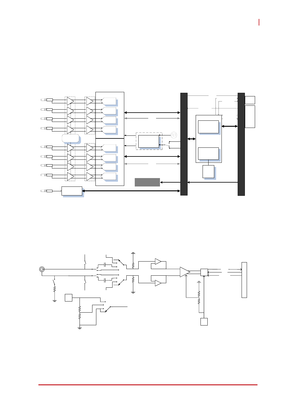
This chapter contains information regarding analog input, trigger-
ing and timing for the PXIe-9529.
3.1 Functional Block Diagram
3.2 Analog Input Channel
3.2.1
Analog Input Front-End Configuration
Figure 3-1: Analog Input Architecture
CLK100p/n,
PXIe_DSTARAp/n
CLK
Synthesizer
Reference &
Calibration
10 MHz
2-bit /12.288MHz
TRG IN
Bo
a
rd t
o
Bo
a
rd C
o
nn
x
2
ADC Ctrl
CH0
Quad
24bit ADC
ADC
ADC
ADC
ADC
ADC
ADC
ADC
ADC
CH1
CH2
CH3
CH4
CH5
CH6
CH7
PGA
PGA
CLK100p/n
2-bit / 12.288MHz
ADC Ctrl
IO
Control
DC-DC\
LDO
JFET Buffer
OPAMP
3.3V
5V
12V
FPGA
ADC Control
Trigger Control
Data Processing
FIFO Interface
PCIe Controller
PCIe Gen1
x4
DDR2
512MB
Memory
PXI
e Hyb
rid P
e
riph
eral Sl
ot
XJ4
XJ3
ADC
BUS
PXIe_DSTARCp/n
SYNC100p/n,
PXIe_DSTARBp/n
Trigger Bus [0..7]
Geographical Address [0..4]
PXI CLK10
PXI CLK10
3.3V
5V
12V
Quad
24bit ADC
BUF
BUF
PGA
PGA
BUF
BUF
BUF
BUF
BUF
BUF
PGA
PGA
PGA
PGA
PGA
PGA
24-bit ADC
JFET OPAMP
JFET OPAMP
330nF / 25V
CAL+
CAL-
IEPE-
1MR
1MR
330nF / 25V
SPST
SPST
IEPE+
49.9R
SPST
CARR
DATA
ADC Ctrl
SCK
Vref
Vref
10k
10k
10k
10k
Cal+
PGA
Signal Switch
X1
X10