5 adc timing control, 1 timebase architecture, Adc timing control – ADLINK PXIe-9848 User Manual
Page 35: Timebase architecture, Figure 3-11, Re-trigger mode acquisition, Figure 3-12, Pxie-9848 timebase architecture
Operations
25
PXIe-9848
3.4.5
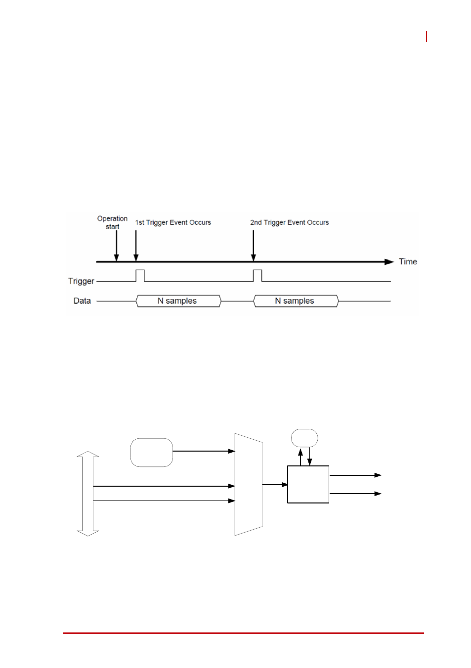
Post-Trigger or Delayed-Trigger Acquisition with
Re-Triggering
Post-trigger or delayed trigger acquisition with re-triggering are
applicable to collect data after several trigger events, as shown.
Once the number of triggers has been programmed, the digitizer
acquires a specific data sample each time a trigger is accepted.
The time between a previous sample and subsequent trigger
event can only be one Timebase clock period. Following initial
setup, the process requires no additional software intervention.
Figure 3-11: Re-Trigger Mode Acquisition
3.5 ADC Timing Control
3.5.1
Timebase Architecture
Figure 3-12: PXIe-9848 Timebase Architecture
The PXIe-9848 supports the following timebase sources for ana-
log input conversion.
Timebase C
lock Switch
PXIe Interface
PXIe_CLK100
PXI_CLK10
Onboard
Oscillator
10M
ADC0
ADC1
VCXO
100M
Multiplier
PLL
Synthesizer