3 operations, 1 functional block diagram, 2 analog input channel – ADLINK PXIe-9848 User Manual
Page 23: 1 analog input front-end configuration, Functional block diagram, Analog input channel, Analog input front-end configuration, Figure 3-1, Analog input architecture of the pxie-9848, 3operations
Operations
13
PXIe-9848
3
Operations
This chapter contains information regarding analog input, analog
output, triggering and timing for the PXIe-9848, as well as data
transfer and multiple module synchronization functions.
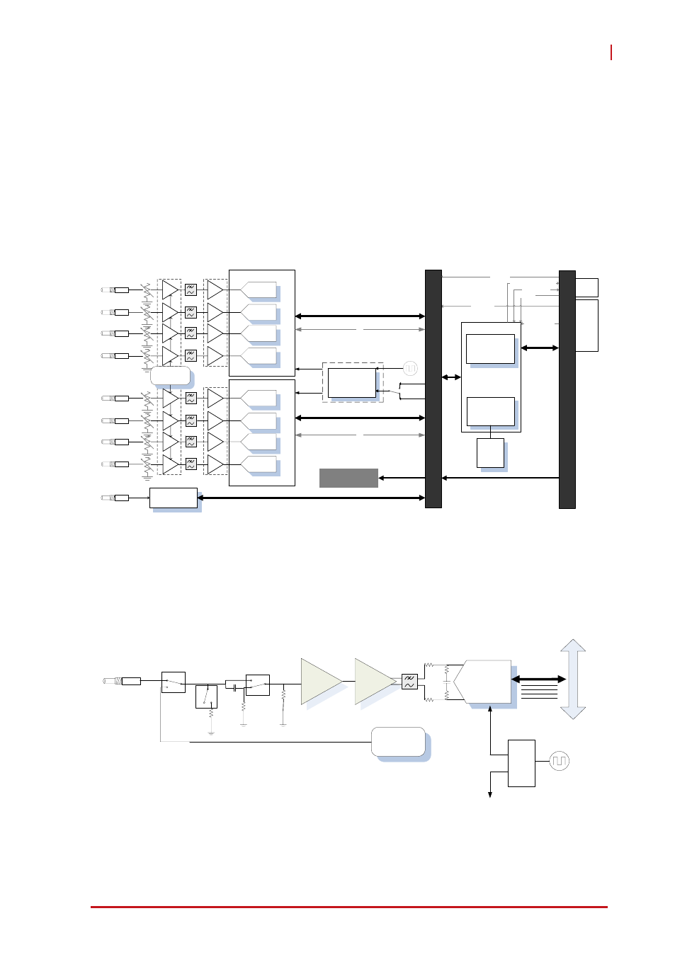
3.1 Functional Block Diagram
3.2 Analog Input Channel
3.2.1
Analog Input Front-End Configuration
Figure 3-1: Analog Input Architecture of the PXIe-9848
PXIe_CLK100
PLL CLK
Synthesizer
Reference &
Calibration
10 MHz
8-bit / 200MHz
TRG IN
Board to Board Conn x2
SPI
CH0
Quad
14bit 100MSps
ADC
BUF
VGA
BUF
VGA
ADC
ADC
BUF
VGA
BUF
VGA
BUF
VGA
BUF
VGA
BUF
VGA
BUF
VGA
ADC
ADC
ADC
ADC
ADC
ADC
CH1
CH2
CH3
CH4
CH5
CH6
CH7
High Speed
VGA
CLK100p/n
8-bit / 200MHz
SPI
Input
Control
DC-DC\
LDO
JFET OP
Buffer
3.3V
5V
12V
FPGA
ADC Control
Trigger Control
Data Processing
PCIe Controller
PCIe Gen1
x4
DDR2
512MB
Memory
PXIe Hybrid Peripheral Slot
XJ4
XJ3
ADC
BUS
PXIe_DSTARBp/n
Trigger Bus [0..7]
Geographical Address [0..4]
PXI_CLK10
PXI CLK10
3.3V
5V
12V
Quad
14bit 100MSps
ADC
High Speed
VGA
PXI_STAR
Quad
14bit 100MSps
ADC
+2.5V
Reference
&
Calibration
10 MHz
Board
to Boa
rd
Bus
CH0
JF
ET
OP
Bu
ffe
r
50ohm
Relay
Relay
1Mohm
1Gohm
Relay
Hi
gh
Sp
ee
d
VG
A
CLK
GEN
AD9523
Relay