2 input range and data format, Input range and data format – ADLINK PXIe-9848 User Manual
Page 25
Operations
15
PXIe-9848
3.2.2
Input Range and Data Format
A/D acquisition is initiated by a trigger source, which must be pre-
determined. Data acquisition will commence once the trigger con-
dition is established. Following completion of A/D conversion, A/D
data is buffered in a Data FIFO, and can then be transferred to PC
memory for further processing.
Data format of the PXIe-9848 is 2’s complement. The ADC data of
the PXIe-9848 is on the 14 MSB of the 16-bit A/D data. The 2 LSB
of the 16-bit A/D data should be truncated by software. A/D data
structure is as follows.
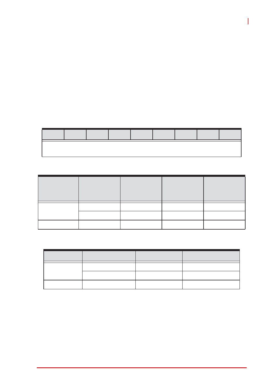
Table 3-1: Input Range and Data Format
Table 3-2: Input Range FSR and –FSR Values
Table 3-3: Input Range Midscale Values
D15
D14
D13
D12
….
D3
D2
D1
D0
D15 ~ D2 bits represent the data from ADC CHx (2’s complement)
D1, D0 bits are identical to D2 bit and should be truncated.
Description
Full-scale
range
Least
significant
bit
FSR-1LSB
-FSR
Bipolar
Analog Input
±2 V
244.14 μV
1.999756 V
-2 V
±0.2V
24.41 μV
0.199975 V
-0.2 V
Digital Code
N/A
N/A
7FFF
8000
Description Midscale +1LSB
Midscale
Midscale –1LSB
Bipolar
Analog Input
244
µV
0 V
-244
µV
24.41 μV
0 V
-24.41 μV
Digital Code
0001
0000
FFFF