Acrosser AR-B1894 User Manual
Page 31

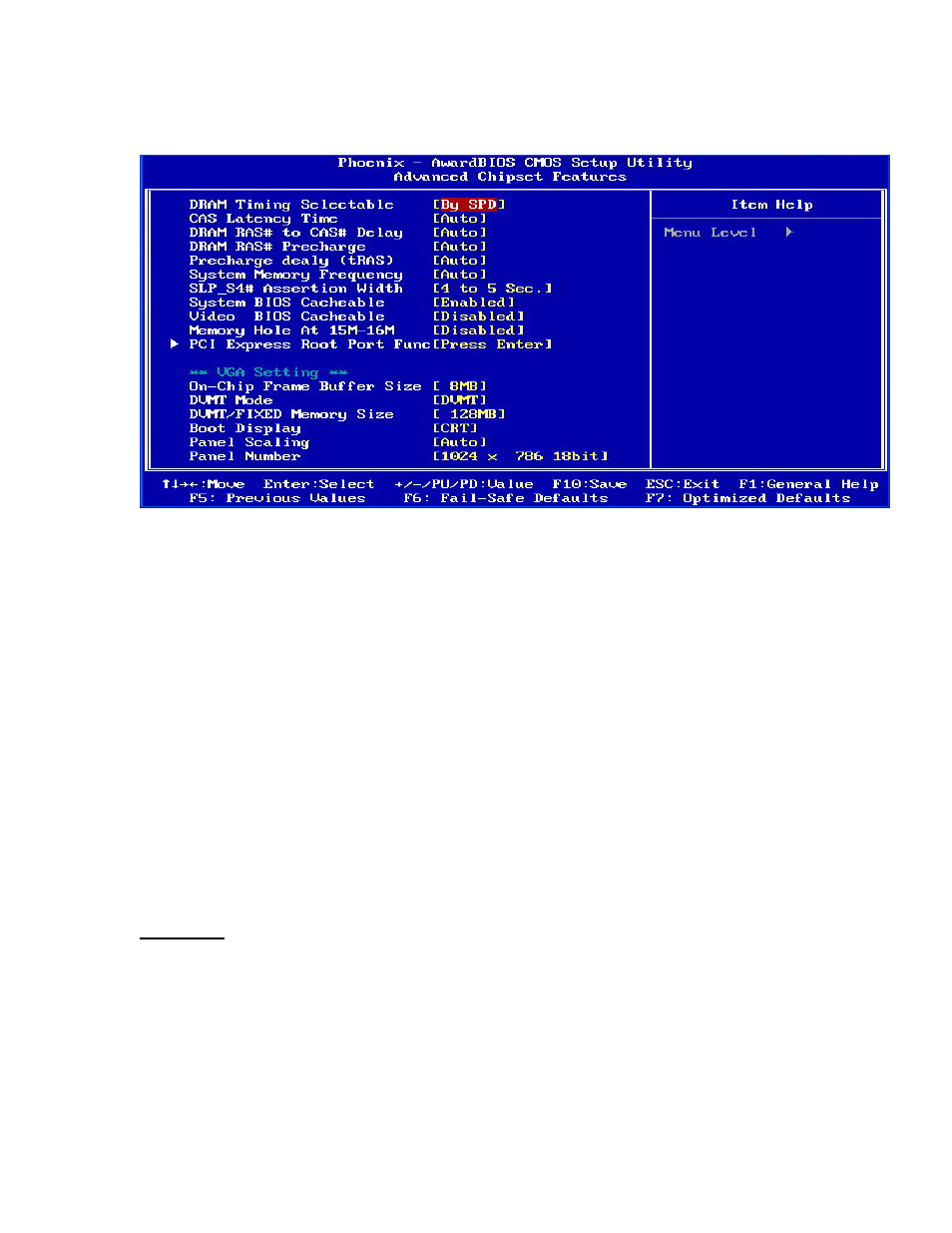
4.2.3Advanced Chipset Features
4.2.3.1 DRAM Timing Selectable
This item determines DRAM clock/timing using SPD or manual configuration.
Make sure your memory module has SPD (Serial Presence Data), if you want to
select the “By SPD” option. Options: Manual、By SPD (default)
4.2.3.2 CAS Latency Time
CAS is short for column address strobe, which is a kind of signals. When the
CPU needs data from SDRAM, CAS signals will be sent via the CAS line to
specify the column where the data is needed. This controls the time delay (in
clock cycles - CLKs) that passes before the SDRAM starts to carry out a read
command after receiving it. This also determines the number of CLKs for the
completion of the first part of a burst transfer. In other words, the lower the
latency, the faster the transaction.
Note that some SDRAM modules may not be able to handle the lower latency
and will become unstable and lose data. Therefore, set the DRAM CAS Latency
Time to 2 for optimal performance if possible but increase it to 2.5 if your system
becomes unstable.
Interestingly, increasing the CAS latency time does have an advantage in that it
will enable the SDRAM to run at a higher clockspeed, thereby giving you an edge
in overclocking your system. So, if you hit a snag while overclocking, try
increasing the CAS latency time.
4.2.3.3 DRAM RAS# to CAS# Delay
This item allows you to select a delay time between the CAS and RAS strobe
signals. It only applies when DRAM is written to, read from, or refreshed. This
field is adjustable only when “DRAM Timing Selectable” is set to “manual”. This
field is locked when “DRAM Timing Selectable” is set to “By SPD” and is
automatically determined by the system. Options: 5、4、3、2.
