Acrosser AR-B1894 User Manual
Page 17
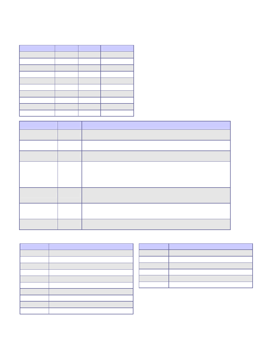
2.3.8 DVI Connector (DVI
Description
PIN No.
PIN No.
Description
TDC0#
2
1
+5V
TDC0 4 3 GND
NC
6
5
NC
NC 8
7 NC
TDC1#
10
9
HPDET
TDC1 12
11
MDVIDATA
NC
14
13
MDVICLK
NC 16
15
Ground
TDC2#
18
17
TLC#
TDC2 20
19 TLC
Signal
Type
Description
TDC0,TDC0#
O
DVI Data Channel 0 Output
: These pins provide the DVI differential
output for data channel 0 (Blue).
TDC1,TDC1#
O
DVI Data Channel 1 Output
: These pins provide the DVI differential
output for data channel 1 (Green).
TDC2,TDC2#
O
DVI Data Channel 2 Output
: These pins provide the DVI differential
output for data channel 2 (Red).
HPDET
I
Hot Plug Detect (internal pull-down)
: This input determines whether the
DVI is connected to a DVI monitor. When terminated , the monitor is
required to apply a voltage greater than 2.4 volts. Changes on the status
of this pin will be relayed to the graphics controller via the P-OUT/TLDET*
or GPIO(1)/TLDET* pin pulling low.
TMDSDATA
I/O
DVI I2C Data
: This signal is used as the I2C DOC clock for a digital
display connector (i.e. TV-Out Encoder , TMDS transmitter ). This signal
is tri-stated during a hard reset.
TMDSDCLK
I/O
DVI DOC Clock
: This signal is used as the DOC clock for a digital display
connector (i.e. primary digital monitor). This signal is tri-stated during a
hard reset.
TLC,TLC#
O
DVI Clock Output:
These pins provide the differential clock outputs to the
DVI interface corresponding a data on TDC(0:2) outputs.
2.3.9 GPIO Connector (GPIO1)
2.3.10 IrDA Connector (IR1)
PIN No.
Description
1
+3.3V
2
General Purpose I/O bit 3
3
General Purpose I/O bit 5
4
General Purpose I/O bit 0
5
General Purpose I/O bit 7
6
General Purpose I/O bit 2
7
General Purpose I/O bit 4
8
General Purpose I/O bit 1
9
General Purpose I/O bit 6
10 Ground
PIN No.
Description
1
NC
2 NC
3
+5V
4
Infrared transmitter output
5
Ground
6
Infrared receiver input