Switching waveforms – Cypress CY7C140 User Manual
Page 10
CY7C130, CY7C130A
CY7C131, CY7C131A
CY7C140, CY7C141
Document #: 38-06002 Rev. *E
Page 10 of 19
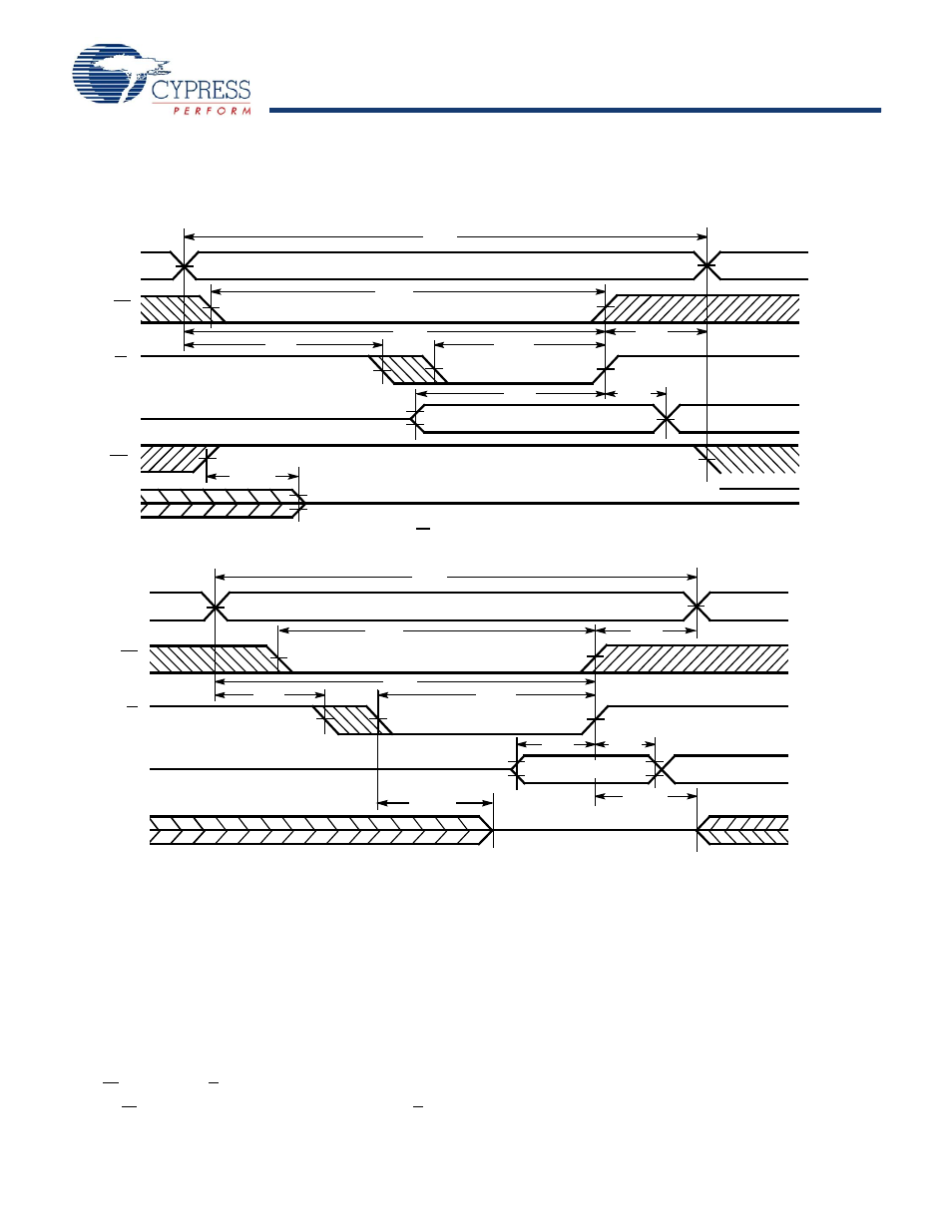
Figure 8. Write Cycle No. 1 (OE Three-States Data I/Os—Either Port
Figure 9. Write Cycle No. 2 (R/W Three-States Data I/Os—Either Port)
Switching Waveforms
(continued)
t
AW
t
WC
DATA VALID
HIGH IMPEDANCE
t
SCE
t
SA
t
PWE
t
HD
t
SD
t
HA
CE
R/W
ADDRESS
t
HZOE
OE
D
OUT
DATA
IN
Either Port
t
AW
t
WC
t
SCE
t
SA
t
PWE
t
HD
t
SD
t
HZWE
t
HA
HIGH IMPEDANCE
DATA VALID
t
LZWE
ADDRESS
CE
R/W
DATA
OUT
DATA
IN
Notes
23. If OE is LOW during a R/W controlled write cycle, the write pulse width must be the larger of t
PWE
or t
HZWE
+ t
SD
to allow the data I/O pins to enter high impedance
and for data to be placed on the bus for the required t
SD
.
24. If the CE LOW transition occurs simultaneously with or after the R/W LOW transition, the outputs remain in the high impedance state.