Pin definitions – Cypress CY14B108L User Manual
Page 3
ADVANCE
CY14B108L, CY14B108N
Document Number: 001-45523 Rev. *A
Page 3 of 20
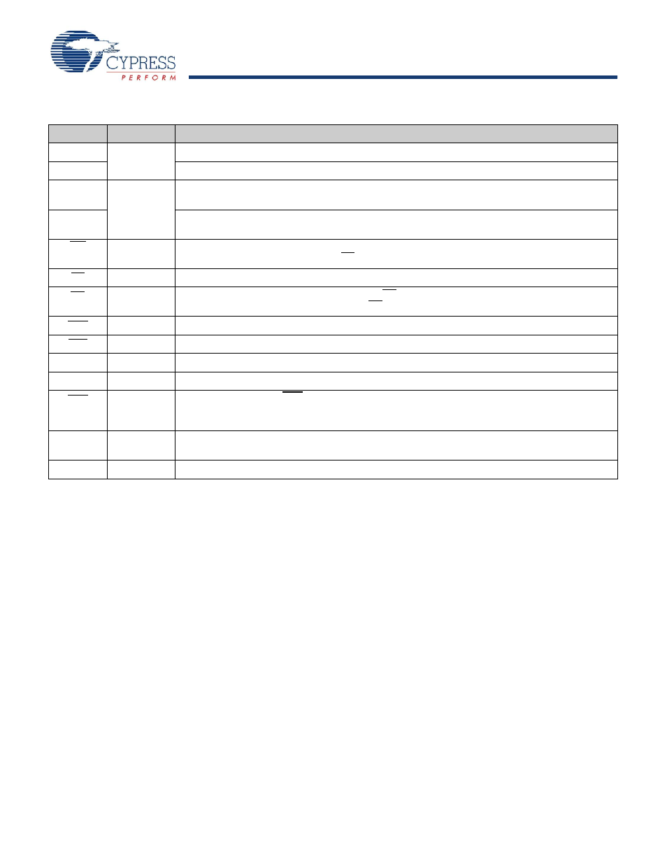
Pin Definitions
Pin Name
IO Type
Description
A
0
– A
19
Input
Address Inputs Used to Select One of the 1,048,576 bytes of the nvSRAM for x8 Configuration.
A
0
– A
18
Address Inputs Used to Select One of the 524, 288 bytes of the nvSRAM for x16 Configuration.
DQ0 – DQ7
Input/Output
Bidirectional Data IO Lines for x8 Configuration. Used as input or output lines depending on
operation.
DQ0 – DQ15
Bidirectional Data IO Lines for x16 Configuration. Used as input or output lines depending on
operation.
WE
Input
Write Enable Input, Active LOW. When selected LOW, data on the IO pins is written to the address
location latched by the falling edge of CE.
CE
Input
Chip Enable Input, Active LOW. When LOW, selects the chip. When HIGH, deselects the chip.
OE
Input
Output Enable, Active LOW. The active LOW OE input enables the data output buffers during read
cycles. IO pins are tri-stated on deasserting OE high.
BHE
Input
Byte High Enable, Active LOW. Controls DQ15 - DQ8.
BLE
Input
Byte Low Enable, Active LOW. Controls DQ7 - DQ0.
V
SS
Ground
Ground for the Device. Must be connected to the ground of the system.
V
CC
Power Supply Power Supply Inputs to the Device.
HSB
Input/Output
Hardware Store Busy (HSB). When LOW this output indicates that a hardware store is in progress.
When pulled LOW external to the chip it initiates a nonvolatile STORE operation. A weak internal pull
up resistor keeps this pin HIGH if not connected (connection optional).
V
CAP
Power Supply AutoStore Capacitor. Supplies power to the nvSRAM during power loss to store data from the SRAM
to nonvolatile elements.
NC
No Connect
No Connect. Do not connect this pin to the die.