Preventing store, Best practices, Stk22c48 – Cypress STK22C48 User Manual
Page 5
STK22C48
Document Number: 001-51000 Rev. **
Page 5 of 14
Preventing Store
The STORE
function is disabled by holding HSB high with a
driver capable of sourcing 30 mA at a V
OH
of at least 2.2V,
because it must overpower the internal pull down device. This
device drives HSB LOW for 20 ns at the onset of a STORE.
When the STK22C48 is connected for AutoStore operation
(system V
CC
connected to V
CC
and a 68
μF capacitor on V
CAP
)
and V
CC
crosses V
SWITCH
on the way down, the STK22C48
attempts to pull HSB LOW. If HSB does not actually get below
V
IL
, the part stops trying to pull HSB LOW and abort the STORE
attempt.
Best Practices
nvSRAM products have been used effectively for over 15 years.
While ease of use is one of the product’s main system values,
experience gained working with hundreds of applications has
resulted in the following suggestions as best practices:
■
The nonvolatile cells in an nvSRAM are programmed on the
test floor during final test and quality assurance. Incoming
inspection routines at customer or contract manufacturer’s
sites sometimes reprogram these values. Final NV patterns are
typically repeating patterns of AA, 55, 00, FF, A5, or 5A. The
end product’s firmware should not assume that an NV array is
in a set programmed state. Routines that check memory
content values to determine first time system configuration,
cold or warm boot status, and so on must always program a
unique NV pattern (for example, complex 4-byte pattern of 46
E6 49 53 hex or more random bytes) as part of the final system
manufacturing test to ensure these system routines work
consistently.
■
Power up boot firmware routines should rewrite the nvSRAM
into the desired state. While the nvSRAM is shipped in a preset
state, best practice is to again rewrite the nvSRAM into the
desired state as a safeguard against events that might flip the
bit inadvertently (program bugs, incoming inspection routines,
and so on).
■
The V
CAP
value specified in this data sheet includes a minimum
and a maximum value size. The best practice is to meet this
requirement and not exceed the maximum V
CAP
value because
the higher inrush currents may reduce the reliability of the
internal pass transistor. Customers who want to use a larger
V
CAP
value to make sure there is extra store charge should
discuss their V
CAP
size selection with Cypress.
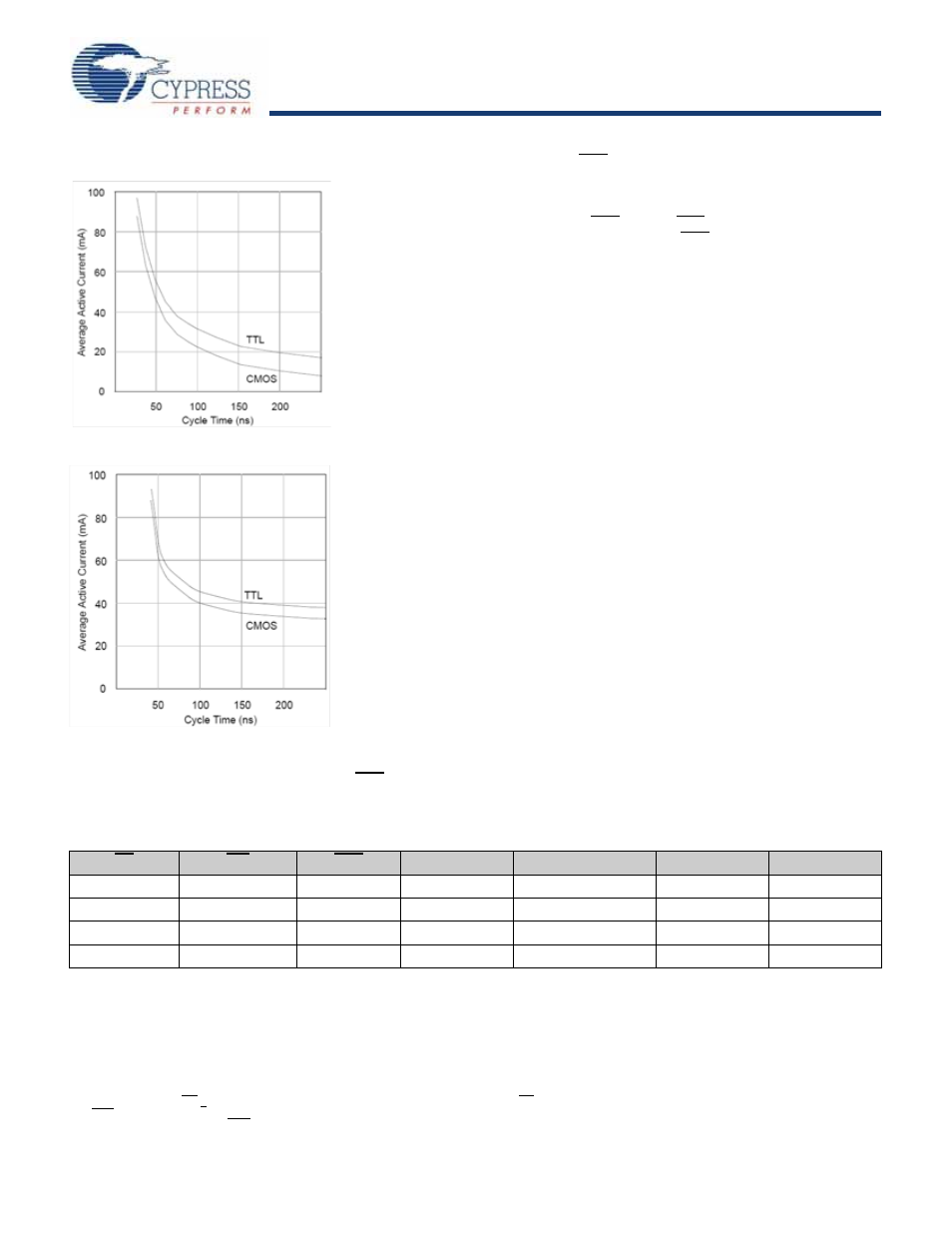
Figure 4. Current Versus Cycle Time (Read)
Figure 5. Current Versus Cycle Time (Write)
Table 2. Hardware Mode Selection
CE
WE
HSB
A10–A0
Mode
IO
Power
H
X
H
X
Not Selected
Output High Z
Standby
L
H
H
X
Read SRAM
Output Data
Active
[1]
L
L
H
X
Write SRAM
Input Data
Active
X
X
L
X
Nonvolatile STORE
Output High Z
I
CC2
Notes
1. I/O state assumes OE < V
IL
. Activation of nonvolatile cycles does not depend on state of OE.
2. HSB STORE operation occurs only if an SRAM Write is done since the last nonvolatile cycle. After the STORE (If any) completes, the part goes into standby mode,
inhibiting all operations until HSB rises.