Tap controller – Cypress CY7C1292DV18 User Manual
Page 12

CY7C1292DV18
CY7C1294DV18
Document #: 001-00350 Rev. *A
Page 12 of 23
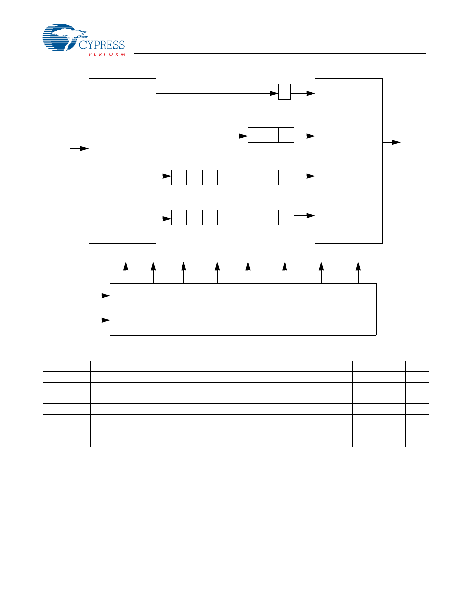
TAP Controller Block Diagram
0
0
1
2
.
.
29
30
31
Boundary Scan Register
Identification Register
0
1
2
.
.
.
.
106
0
1
2
Instruction Register
Bypass Register
Selection
Circuitry
Selection
Circuitry
TAP Controller
TDI
TDO
TCK
TMS
TAP Electrical Characteristics
Over the Operating Range
[10, 11, 12]
Parameter
Description
Test Conditions
Min.
Max.
Unit
V
OH1
Output HIGH Voltage
I
OH
=
−2.0 mA
1.4
V
V
OH2
Output HIGH Voltage
I
OH
=
−100 µA
1.6
V
V
OL1
Output LOW Voltage
I
OL
= 2.0 mA
0.4
V
V
OL2
Output LOW Voltage
I
OL
= 100
µA
0.2
V
V
IH
Input HIGH Voltage
0.65V
DD
V
DD
+ 0.3
V
V
IL
Input LOW Voltage
–0.3
0.35V
DD
V
I
X
Input and OutputLoad Current
GND
≤ V
I
≤ V
DD
−5
5
µA
Notes:
10. These characteristic pertain to the TAP inputs (TMS, TCK, TDI and TDO). Parallel load levels are specified in the Electrical Characteristics table.
11. Overshoot: V
IH
(AC) < V
DDQ
+0.85V (Pulse width less than t
CYC
/2), Undershoot: V
IL
(AC) > –1.5V (Pulse width less than t
CYC
/2).
12. All voltage referenced to Ground.
