Cypress CY7C1231H User Manual
Page 5
CY7C1231H
Document #: 001-00207 Rev. *B
Page 5 of 12
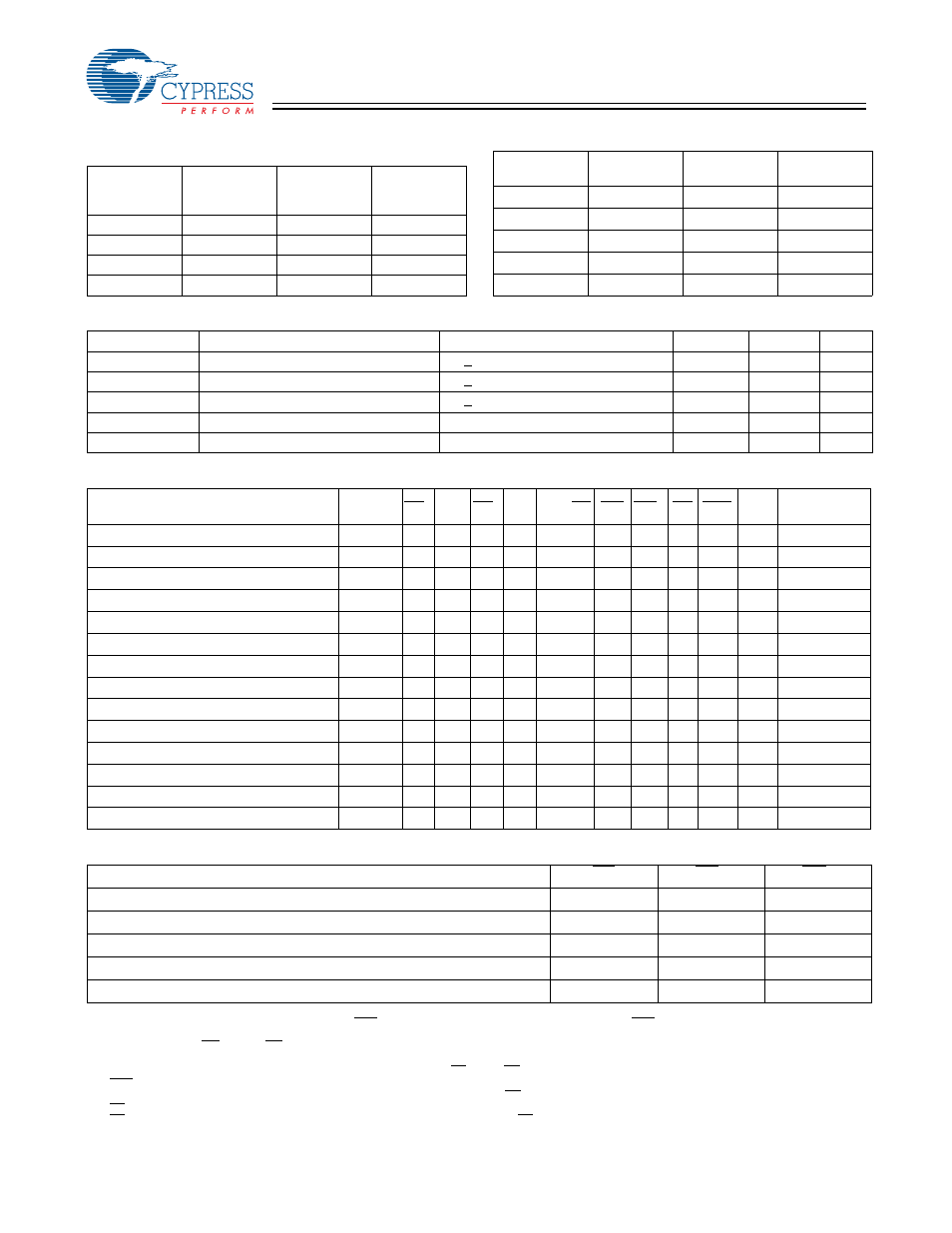
Linear Burst Address Table (MODE = GND)
First
Address
A1, A0
Second
Address
A1, A0
Third
Address
A1, A0
Fourth
Address
A1, A0
00
01
10
11
01
10
11
00
10
11
00
01
11
00
01
10
Interleaved Burst Sequence
First
Address
Second
Address
Third
Address
Fourth
Address
A1, A0
A1, A0
A1, A0
A1, A0
00
01
10
11
01
00
11
10
10
11
00
01
11
10
01
00
ZZ Mode Electrical Characteristics
Parameter
Description
Test Conditions
Min.
Max.
Unit
I
DDZZ
Sleep mode standby current
ZZ > V
DD
− 0.2V
40
mA
t
ZZS
Device operation to ZZ
ZZ > V
DD
− 0.2V
2t
CYC
ns
t
ZZREC
ZZ recovery time
ZZ < 0.2V
2t
CYC
ns
t
ZZI
ZZ Active to sleep current
This parameter is sampled
2t
CYC
ns
t
RZZI
ZZ inactive to exit sleep current
This parameter is sampled
0
ns
Truth Table
[2, 3, 4, 5, 6, 7, 8]
Operation
Address
Used
CE
1
CE2 CE
3
ZZ ADV/LD WE BW
X
OE CEN CLK
DQ
Deselect Cycle
None
H
X
X
L
L
X
X
X
L
L->H
Tri-State
Deselect Cycle
None
X
X
H
L
L
X
X
X
L
L->H
Tri-State
Deselect Cycle
None
X
L
X
L
L
X
X
X
L
L->H
Tri-State
Continue Deselect Cycle
None
X
X
X
L
H
X
X
X
L
L->H
Tri-State
READ Cycle (Begin Burst)
External
L
H
L
L
L
H
X
L
L
L->H Data Out (Q)
READ Cycle (Continue Burst)
Next
X
X
X
L
H
X
X
L
L
L->H Data Out (Q)
NOP/DUMMY READ (Begin Burst)
External
L
H
L
L
L
H
X
H
L
L->H
Tri-State
DUMMY READ (Continue Burst)
Next
X
X
X
L
H
X
X
H
L
L->H
Tri-State
WRITE Cycle (Begin Burst)
External
L
H
L
L
L
L
L
X
L
L->H
Data In (D)
WRITE Cycle (Continue Burst)
Next
X
X
X
L
H
X
L
X
L
L->H
Data In (D)
NOP/WRITE ABORT (Begin Burst)
None
L
H
L
L
L
L
H
X
L
L->H
Tri-State
WRITE ABORT (Continue Burst)
Next
X
X
X
L
H
X
H
X
L
L->H
Tri-State
IGNORE CLOCK EDGE (Stall)
Current
X
X
X
L
X
X
X
X
H
L->H
–
Sleep MODE
None
X
X
X
H
X
X
X
X
X
X
Tri-State
Truth Table for Read/Write
[2, 3]
Function
WE
BW
A
BW
B
Read
H
X
X
Write – No bytes written
L
H
H
Write Byte A – (DQ
A
and
DQP
A
)
L
H
H
Write Byte B – (DQ
B
and
DQP
B
)
L
H
H
Write All Bytes
L
L
L
Notes:
2. X = “Don't Care.” H = Logic HIGH, L = Logic LOW. BWx = 0 signifies at least one Byte Write Select is active, BWx = Valid signifies that the desired byte write
selects are asserted, see Truth Table for details.
3. Write is defined by BW
[A:B]
, and WE. See Truth Table for Read/Write.
4. When a write cycle is detected, all I/Os are tri-stated, even during byte writes.
5. The DQs and DQP
[A:B]
pins are controlled by the current cycle and the OE signal. OE is asynchronous and is not sampled with the clock.
6. CEN = H, inserts wait states.
7. Device will power-up deselected and the I/Os in a tri-state condition, regardless of OE.
8. OE is asynchronous and is not sampled with the clock rise. It is masked internally during write cycles. During a read cycle DQs and DQP
[A:B]
= Tri-state when
OE is inactive or when the device is deselected, and DQs and DQP
[A:B]
= data when OE is active.